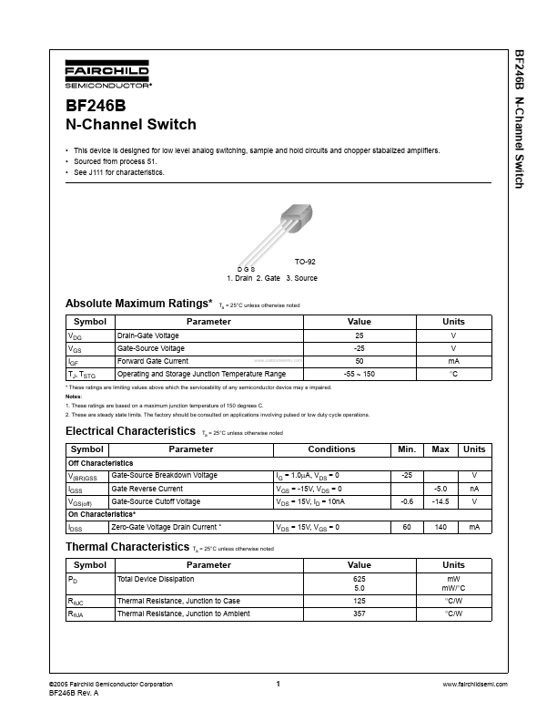
The following content is an automatically extracted verbatim text
from the original manufacturer datasheet and is provided for reference purposes only.
View original datasheet text
BF246B N-Channel Switch
BF246B
N-Channel Switch
• This device is designed for low level analog switching, sample and hold circuits and chopper stabalized amplifiers. • Sourced from process 51. • See J111 for characteristics.
TO-92
DGS
1. Drain 2. Gate 3. Source
Absolute Maximum Ratings*
Symbol
VDG VGS IGF TJ, TSTG
Notes:
Ta = 25°C unless otherwise noted
Parameter
Drain-Gate Voltage Gate-Source Voltage Forward Gate Current
www.DataSheet4U.com
Value
25 -25 50 -55 ~ 150
Units
V V mA °C
Operating and Storage Junction Temperature Range
* These ratings are limiting values above which the serviceability of any semiconductor device may e impaired. 1. These ratings are based on a maximum junction temperature of 150 degrees C. 2. These are steady state limits.