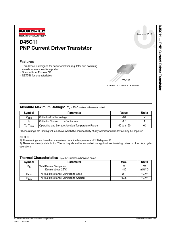
This device is designed for power amplifier, regulator and switching circuits where speed is important.
Sourced from Process 5P.
NZT751 for characteristics. 1
TO-220
1. Base 2. Collector 3. Emitter
Absolute Maximum Ratings.
TA = 25°C unless otherwise noted
Symbol
Parameter
Value
Units
VCEO IC
TJ, TSTG
Collector-Emitter Voltage Collector Current - Continuous Operating and Storage Junction Temperature Range
-80
V
-4.0
A
-55 to +150
°C.
Full PDF Text Transcription for D45C11 (Reference)
Note: Below is a high-fidelity text extraction (approx. 800 characters) for
D45C11. For precise diagrams, and layout, please refer to the original PDF.
D45C11 — PNP Current Driver Transistor D45C11 PNP Current Driver Transistor January 2010 Features • This device is designed for power amplifier, regulator and switching c...
View more extracted text
This device is designed for power amplifier, regulator and switching circuits where speed is important. • Sourced from Process 5P. • NZT751 for characteristics. 1 TO-220 1. Base 2. Collector 3. Emitter Absolute Maximum Ratings* TA = 25°C unless otherwise noted Symbol Parameter Value Units VCEO IC TJ, TSTG Collector-Emitter Voltage Collector Current - Continuous Operating and Storage Junction Temperature Range -80 V -4.0 A -55 to +150 °C *These ratings are limiting values above which the serviceability of any semiconductor device may be impaired. NOTES: 1) These ratings are based on a maximum junction temperature of 150 deg