FDMA510PZ
Features
General Description
This device is designed specifically for battery charge or load switching in cellular handset and other ultraportable applications. It features a MOSFET with low on-state resistance. The Micro FET 2X2 package offers exceptional thermal performance for its physical size and is well suited to linear mode applications.
- Max r DS(on) = 30mΩ at VGS =
- 4.5V, ID =
- 7.8A
- Max r DS(on) = 37mΩ at VGS =
- 2.5V, ID =
- 6.6A
- Max r DS(on) = 50mΩ at VGS =
- 1.8V, ID =
- 5.5A
- Max r DS(on) = 90mΩ at VGS =
- 1.5V, ID =
- 2.0A
- Low profile
- 0.8mm maximum
- in the new package Micro FET 2X2 mm
- HBM ESD protection level > 3KV typical (Note 3)
- Ro HS pliant
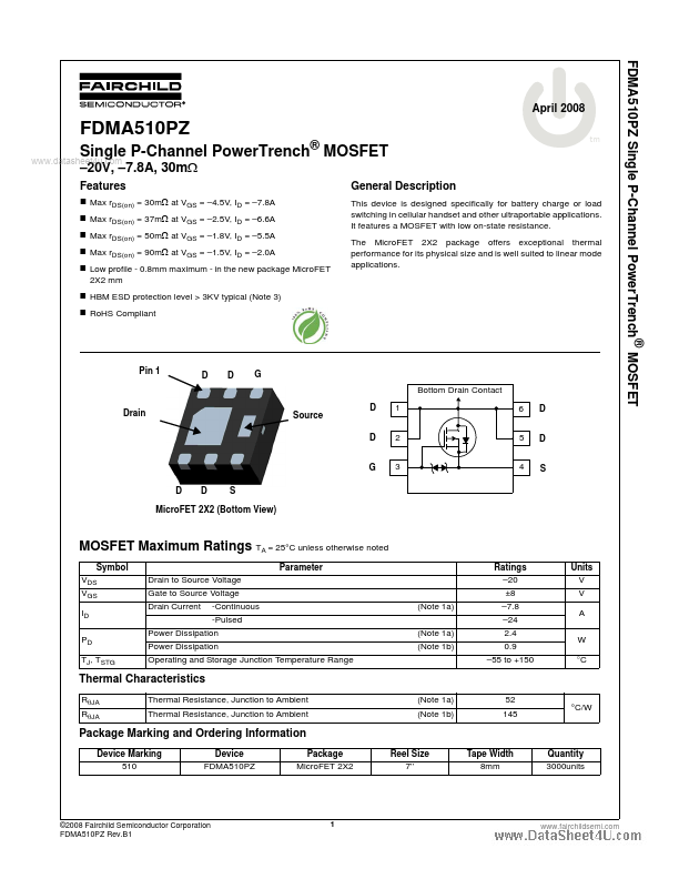
Pin 1
G Bottom Drain Contact
Drain
Source
1 2 3
6 5 4
Micro FET 2X2 (Bottom View)
MOSFET Maximum Ratings TA = 25°C unless otherwise noted
Symbol VDS VGS ID PD TJ, TSTG Parameter Drain to Source Voltage Gate to Source Voltage Drain Current -Continuous -Pulsed Power Dissipation Power Dissipation...