Download FDMB2307NZ Datasheet PDF
Fairchild Semiconductor
FDMB2307NZ
FDMB2307NZ is Dual Common Drain N-Channel MOSFET manufactured by Fairchild Semiconductor.
Features - Max r S1S2(on) = 16.5 mΩ at VGS = 4.5 V, ID = 8 A - Max r S1S2(on) = 18 mΩ at VGS = 4.2 V, ID = 7.4 A - Max r S1S2(on) = 21 mΩ at VGS = 3.1 V, ID = 7 A - Max r S1S2(on) = 24 mΩ at VGS = 2.5 V, ID = 6.7 A - Low Profile - 0.8 mm maximum - in the new package Micro FET 2x3 mm - HBM ESD protection level > 2 k V (Note 3) - Ro HS pliant October 2011 General Description 
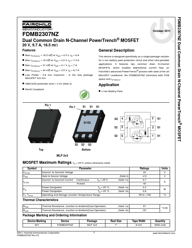
This device is designed specifically as a single package solution for Li-Ion battery pack protection circuit and other ultra-portable applications. It features two mon drain N-channel MOSFETs, which enables bidirectional current flow, on Fairchild’s advanced Power Trench® process with state of the art Micro FET Leadframe, the FDMB2307NZ minimizes both PCB space and r S1S2(on). Application - Li-Ion Battery Pack Pin 1 Pin 1 S1 S1 G1 G2 D1/D2 S2 S2 4 5 G1 2 1 S1 S1 S2 Top S2 G2 Bottom MLP 2x3 MOSFET Maximum Ratings TA = 25°C unless otherwise noted Symbol VS1S2 VGS IS1S2 PD TJ, TSTG Parameter Source1 to Source2 Voltage Gate to Source Voltage Source1 to Source2 Current Power Dissipation Power Dissipation -Continuous -Pulsed TA = 25 °C TA = 25 °C (Note 1a) (Note 1b) TA = 25°C (Note 4) (Note 1a) Ratings 20 ±12 9.7 40 2.2 0.8 -55 to +150 Units V V A W °C Operating and Storage Junction Temperature Range Thermal Characteristics RθJA RθJA Thermal Resistance, Junction to Ambient(Dual Operation) Thermal Resistance, Junction to Ambient(Dual Operation) (Note 1a) (Note 1b) 57 161 °C/W Package Marking and Ordering Information Device Marking 307 Device FDMB2307NZ Package MLP...