FST32211G
FST32211G is 40/48-Bit Bus Switch manufactured by Fairchild Semiconductor.
- Part of the FST comparator family.
FST32211 40/48-Bit Bus Switch
April 2001 Revised July 2002
FST32211 40/48-Bit Bus Switch
General Description
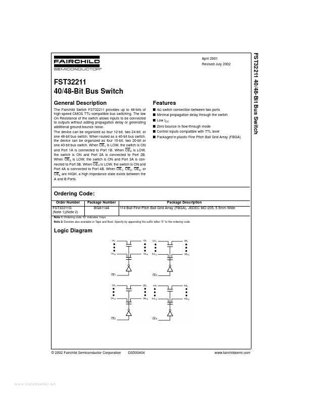
The Fairchild Switch FST32211 provides up to 48-bits of high-speed CMOS TTL-patible bus switching. The low On Resistance of the switch allows inputs to be connected to outputs without adding propagation delay or generating additional ground bounce noise. The device can be organized as four 12-bit, two 24-bit, or one 48-bit bus switch. When routed as a 40-bit bus switch, the device can be organized as four 10-bit, two 20-bit or one 40-bit bus switch. When OE1 is LOW, the switch is ON and Port 1A is connected to Port 1B. When OE2 is LOW, the switch is ON and Port 2A is connected to Port 2B. When OE3 is LOW, the switch is ON and Port 3A is connected to Port 3B. When OE4 is LOW, the switch is ON and Port 4A is connected to Port 4B. When OE1, OE2, OE3, or OE4 are HIGH, a high impedance state exists between the A and B Ports.
Features
I 4Ω switch connection between two ports I Minimal propagation delay through the switch I Low l CC I Zero bounce in flow-through mode I Control inputs patible with TTL level I Packaged in plastic Fine Pitch Ball Grid Array (FBGA)
Ordering Code:
Order Number FST32211G (Note 1)(Note 2) Package Number BGA114A Package Description 114-Ball Fine-Pitch Ball Grid Array (FBGA), JEDEC MO-205, 5.5mm Wide
Note 1: Ordering code “G” indicates Trays. Note 2: Devices also available in Tape and Reel. Specify by appending the suffix letter “X” to the ordering code.
Logic Diagram
© 2002 Fairchild Semiconductor Corporation
DS500404
.fairchildsemi.
..net
FST32211
Connection Diagram
FBGA Pin Assignments
(40-Bit Routing) 1 A B C D E F G H J K L M N P R T U V 1A2 1A4 1A6 1A8 1A10 2A2 2A4 2A6 2A8 2A10 3A9 3A7 3A5 3A3 3A1 4A9 4A7 4A5 4A3 2 1A1 1A3 1A5 1A7 1A9 2A1 2A3 2A5 2A7 3A10 3A8 3A6 3A4 3A2 4A10 4A8 4A6 4A4 4A2 3 NC GND GND GND VCC VCC VCC GND 2A9 GND GND GND VCC VCC GND GND GND 4A1 OE3 4 OE2 OE1 GND GND VCC VCC GND...