J176
J174 / J175 / J176 / J177 / MMBFJ175 / MMBFJ176 / MMBFJ177
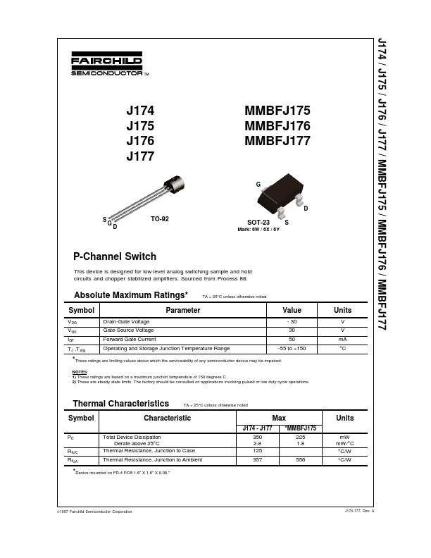
J174 J175 J176 J177
MMBFJ175 MMBFJ176 MMBFJ177
TO-92
SOT-23
Mark: 6W / 6X / 6Y
P-Channel Switch
This device is designed for low level analog switching sample and hold circuits and chopper stabilized amplifiers. Sourced from Process 88.
Absolute Maximum Ratings-
Symbol
VDG VGS IGF TJ ,Tstg Drain-Gate Voltage Gate-Source Voltage Forward Gate Current
TA = 25°C unless otherwise noted
Parameter
Value
- 30 30 50 -55 to +150
Units
V V m A °C
Operating and Storage Junction Temperature Range
- These ratings are limiting values above which the serviceability of any semiconductor device may be impaired.
NOTES: 1) These ratings are based on a maximum junction temperature of 150 degrees C. 2) These are steady state limits. The factory should be consulted on applications involving pulsed or low duty cycle operations.
Thermal Characteristics
Symbol
PD RθJC RθJA
TA = 25°C unless otherwise noted
Characteristic
Total...