J270
Overview
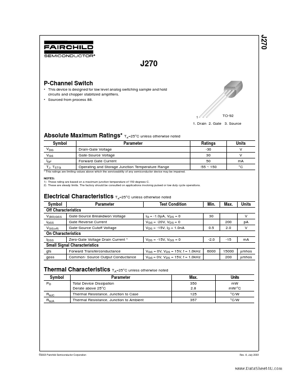
J270 J270 P-Channel Switch • This device is designed for low level analog switching sample and hold circuits and chopper stabilized amplifiers. • Sourced from process 88. 1 TO-92 1. Drain 2. Gate ...
| Part | J270 |
|---|---|
| Description | P-Channel Switch |
| Manufacturer | Fairchild Semiconductor |
| Size | 30.79 KB |
J270 J270 P-Channel Switch • This device is designed for low level analog switching sample and hold circuits and chopper stabilized amplifiers. • Sourced from process 88. 1 TO-92 1. Drain 2. Gate ...