MB8S
MB8S is 0.5A Bridge Rectifiers manufactured by Fairchild Semiconductor.
MB1S
- MB8S
- 0.5 A Bridge Rectifiers
April 2014
MB1S
- MB8S 0.5 A Bridge Rectifiers
Features
- Low-Leakage
- Surge Overload Rating: 35 A peak
- Ideal for Printed Circuit Board
- UL Certified: UL #E258596
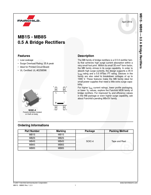
SOIC-4
Polarity symbols molded or mark on body
~~ ++ ~+ ~-
Ordering Informations
Part Number MB1S MB2S MB4S MB6S MB8S
Marking MB1S MB2S MB4S MB6S MB8S
Description
The MB family of bridge rectifiers is a 0.5 A rectifier family that achieves high surge current absorption within a very small foot print. Within its small 35 mm2 form factor, the MB family shines in its surge capability. In order to absorb high surge currents, the design supports a 35 A IFSM rating and a 5.0 A2Sec I2T rating. Devices in the family are also rated to breakdown voltages of up to 1000 V. These Features make the MB family ideal for small power supplies that need a little extra surge capability.
For higher IFAV current ratings, lower profile packaging, or lower VF values, explore the...