SFU2955
FEATURES
Avalanche Rugged Technology Rugged Gate Oxide Technology Lower Input Capacitance Improved Gate Charge Extended Safe Operating Area Lower Leakage Current : 10 µA (Max.) @ VDS = -60V Lower RDS(ON) : 0.22 Ω (Typ.)
SFR/U2955
BVDSS = -60 V RDS(on) = 0.3 Ω ID = -7.6 A
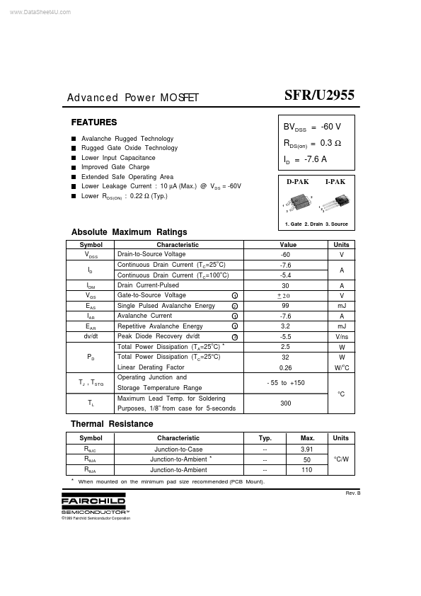
D-PAK
2 1 3
I-PAK
1. Gate 2. Drain 3. Source
Absolute Maximum Ratings
Symbol VDSS ID IDM VGS EAS IAR EAR dv/dt PD Characteristic Drain-to-Source Voltage Continuous Drain Current (TC=25 C) Continuous Drain Current (TC=100 C) Drain Current-Pulsed Gate-to-Source Voltage Single Pulsed Avalanche Energy Avalanche Current Repetitive Avalanche Energy Peak Diode Recovery dv/dt o Total Power Dissipation (TA=25 C)
- o o
Value -60 -7.6 -5.4
1 O 2 O 1 O 1 O 3 O
Units V A A V m J A m J V/ns W W W/ C o
30 + _ 20 99 -7.6 3.2 -5.5 2.5 32 0.26
- 55 to +150
Total Power Dissipation (TC=25 C) Linear Derating Factor Operating Junction and Storage Temperature Range Maximum Lead Temp. for Soldering Purposes, 1/8” from case for...