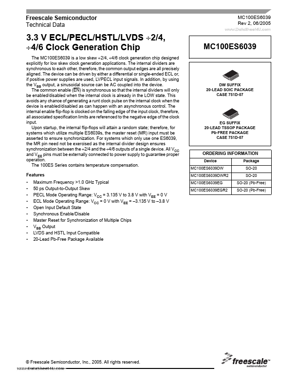
Datasheet4U Logo Datasheet4U.com

MC100ES6039 - 3.3V ECL/PECL/HSTL/LVDS Generation Chip

Datasheet Summary

Description

ECL Diff Clock Inputs ECL Sync Enable ECL Master Reset ECL Reference Output ECL Diff ÷2/4 Outputs ECL Diff ÷4/6 Outputs ECL Freq.

Select Input ÷2/4 ECL Freq.

Features

  • Maximum Frequency >1.0 GHz Typical 50 ps Output-to-Output Skew PECL Mode Operating Range: VCC = 3.135 V to 3.8 V with VEE = 0 V ECL Mode Operating Range: VCC = 0 V with VEE =.
  • 3.135 V to.
  • 3.8 V Open Input Default State Synchronous Enable/Disable Master Reset for Synchronization of Multiple Chips VBB Output LVDS and HSTL Input Compatible 20-Lead Pb-Free Package Available MC100ES603.

📥 Download Datasheet

Datasheet preview – MC100ES6039

Datasheet Details

Part number MC100ES6039
Manufacturer Freescale Semiconductor
File Size 260.61 KB
Description 3.3V ECL/PECL/HSTL/LVDS Generation Chip
Datasheet download datasheet MC100ES6039 Datasheet
Additional preview pages of the MC100ES6039 datasheet.
Other Datasheets by Freescale Semiconductor

Full PDF Text Transcription

Click to expand full text
Freescale Semiconductor Technical Data MC100ES6039 Rev 2, 06/2005 www.DataSheet4U.com 3.3 V ECL/PECL/HSTL/LVDS ÷2/4, ÷4/6 Clock Generation Chip The MC100ES6039 is a low skew ÷2/4, ÷4/6 clock generation chip designed explicitly for low skew clock generation applications. The internal dividers are synchronous to each other, therefore, the common output edges are all precisely aligned. The device can be driven by either a differential or single-ended ECL or, if positive power supplies are used, LVPECL input signals. In addition, by using the VBB output, a sinusoidal source can be AC coupled into the device. The common enable (EN) is synchronous so that the internal dividers will only be enabled/disabled when the internal clock is already in the LOW state.
Published: |