MMA6855QR2 Key Features
- AEC-Q100, Revision G, dated May 14, 2007
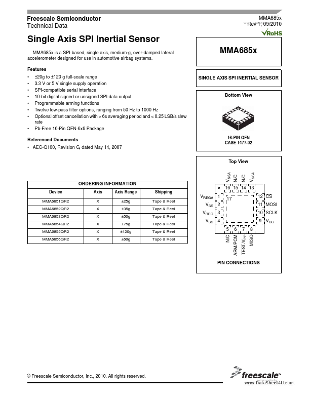
MMA6855QR2 is Single Axis SPI Inertial Sensor manufactured by Freescale Semiconductor.
| Part Number | Description |
|---|---|
| MMA6851QR2 | Single Axis SPI Inertial Sensor |
| MMA6852QR2 | Single Axis SPI Inertial Sensor |
| MMA6853QR2 | Single Axis SPI Inertial Sensor |
| MMA6854QR2 | Single Axis SPI Inertial Sensor |
| MMA6856QR2 | Single Axis SPI Inertial Sensor |
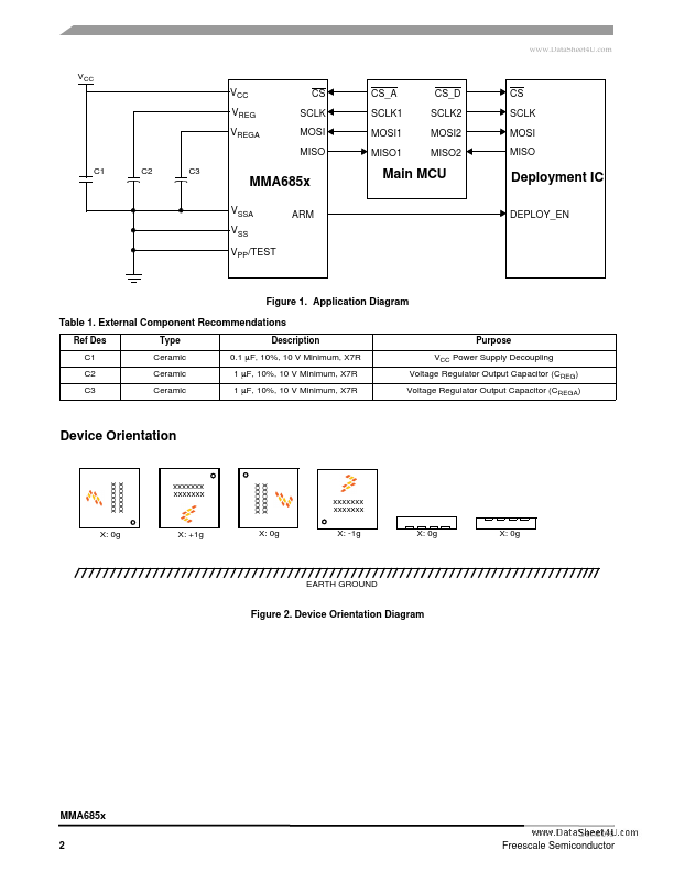
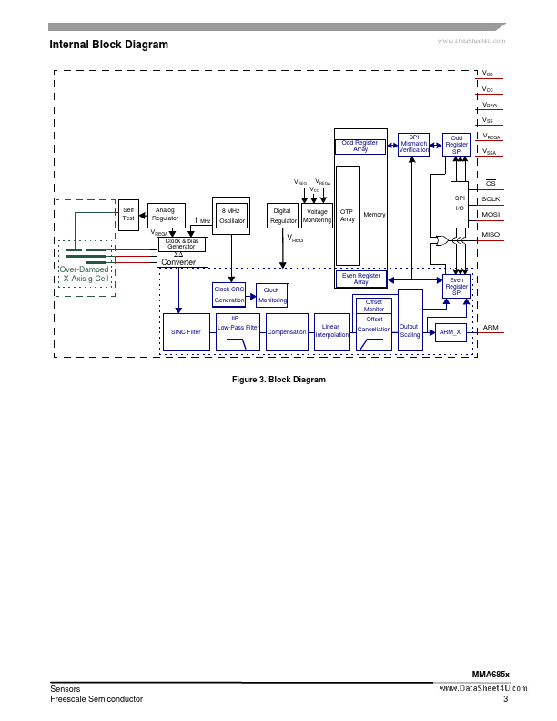
0g MMA685x 2 Sensors Freescale Semiconductor xxxxxxx xxxxxxx X: Device Orientation Diagram xxxxxxx xxxxxxx X: 0g EARTH GROUND Internal Block Diagram.