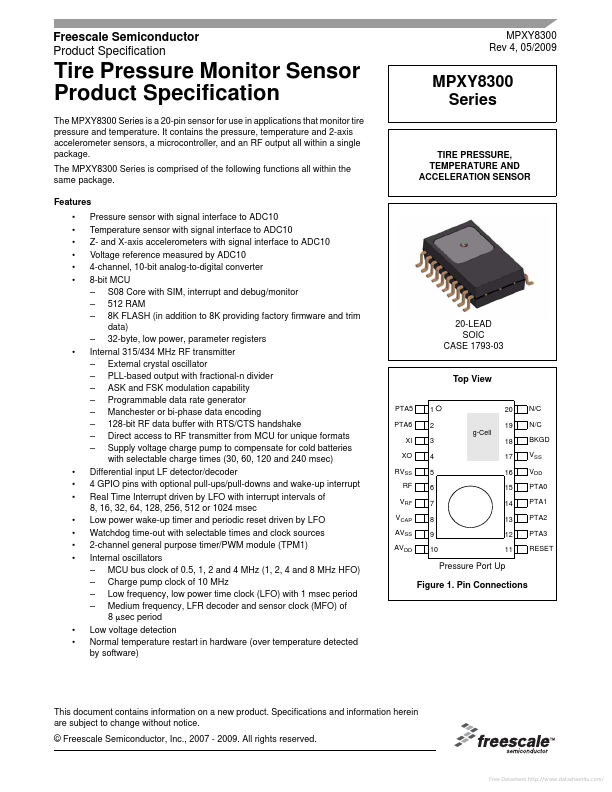
MPXY8300C6U Key Features
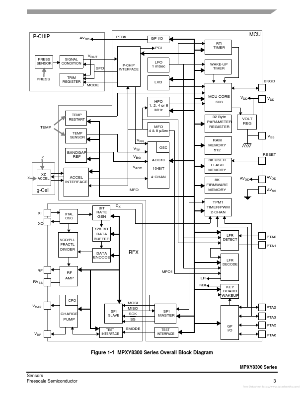
- Pressure sensor with signal interface to ADC10 Temperature sensor with signal interface to ADC10 Z- and X-axis accelerom
- S08 Core with SIM, interrupt and debug/monitor
- 512 RAM
- 8K FLASH (in addition to 8K providing factory firmware and trim data)
- 32-byte, low power, parameter registers Internal 315/434 MHz RF transmitter
- External crystal oscillator
- PLL-based output with fractional-n divider
- ASK and FSK modulation capability
- Programmable data rate generator
- Manchester or bi-phase data encoding


