MRF284LR1 Description
Freescale Semiconductor Technical Data Document Number: 17, 5/2006 RF Power Field Effect Transistors N - Channel Enhancement - Mode Lateral MOSFETs Designed for PCN and PCS base station applications with frequencies from 1000 to 2600 MHz. Suitable for FM, TDMA, CDMA, and multicarrier amplifier applications.
MRF284LR1 Key Features
- Excellent Thermal Stability
- Characterized with Series Equivalent Large
- Signal Impedance Parameters
- Low Gold Plating Thickness on Leads. L Suffix Indicates 40μ″ Nominal
- RoHS pliant
- In Tape and Reel. R1 Suffix = 500 Units per 32 mm, 13 inch Reel. Table 1. Maximum Ratings
- Source Voltage Gate
- Source Voltage Total Device Dissipation @ TC = 25°C Derate above 25°C Storage Temperature Range Case Operating Temperatu
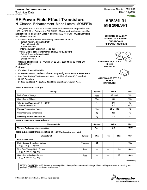
- CHANNEL BROADBAND RF POWER MOSFETs
- 05, STYLE 1 NI