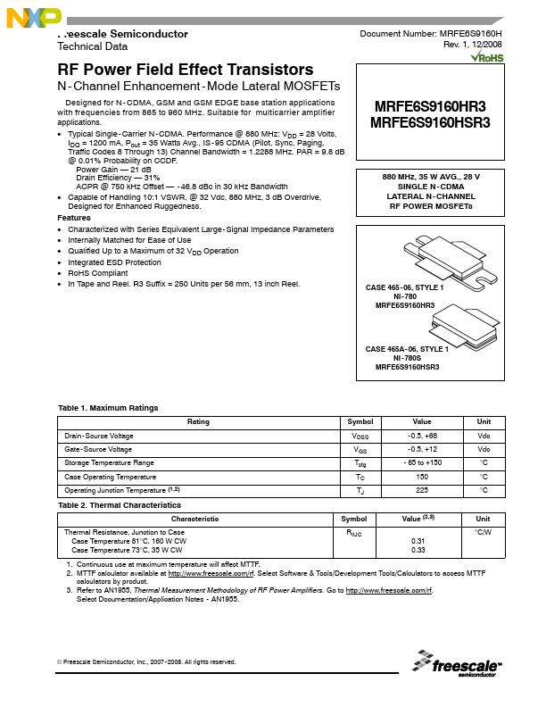
Datasheet4U Logo Datasheet4U.com

MRFE6S9160HR3 - RF Power Field Effect Transistors

General Description

Part Number B1, B2 Ferrite Beads, Small 2743019447 C1, C2, C19 47 pF Chip Capacitors ATC100B470JT500XT C3, C11 0.8- 8.0 pF Variable Capacitors, Gigatrim 27291SL C4 2.7 pF Chip Capacitor ATC100B2R7JT500XT C5, C6 15 pF Chip Capacitors ATC100B150JT500XT C7, C8 12 pF Chip Capacitors A

Key Features

  • Characterized with Series Equivalent Large - Signal Impedance Parameters.
  • Internally Matched for Ease of Use.
  • Qualified Up to a Maximum of 32 VDD Operation.
  • Integrated ESD Protection.
  • RoHS Compliant.
  • In Tape and Reel. R3 Suffix = 250 Units per 56 mm, 13 inch Reel. Document Number: MRFE6S9160H Rev. 1, 12/2008 MRFE6S9160HR3 MRFE6S9160HSR3 880 MHz, 35 W AVG. , 28 V SINGLE N - CDMA.

📥 Download Datasheet

Full PDF Text Transcription for MRFE6S9160HR3 (Reference)

Note: Below is a high-fidelity text extraction (approx. 800 characters) for MRFE6S9160HR3. For precise diagrams, and layout, please refer to the original PDF.

Freescale Semiconductor Technical Data RF Power Field Effect Transistors N - Channel Enhancement - Mode Lateral MOSFETs Designed for N - CDMA, GSM and GSM EDGE base stati...

View more extracted text
ode Lateral MOSFETs Designed for N - CDMA, GSM and GSM EDGE base station applications with frequencies from 865 to 960 MHz. Suitable for multicarrier amplifier applications. • TTIDyrQapfif=cica1lC2So0idn0egmsleA8-,CTPahorruroiteu=rgN3h5-1CW3D)aCMtthsAa.AnPvngee.rl,foBISram-n9ad5nwcCiedDt@hM=A818(.0P22iMlo8Ht8, zSM:yVHnDzc.D, PP=Aa2Rg8in=Vg9o, .l8ts,dB @ 0.01% Probability on CCDF. Power Gain — 21 dB Drain Efficiency — 31% ACPR @ 750 kHz Offset — - 46.8 dBc in 30 kHz Bandwidth • Capable of Handling 10:1 VSWR, @ 32 Vdc, 880 MHz, 3 dB Overdrive, Designed for Enhanced Ruggedness.