FLC057WG
FLC057WG is C-Band Power GaAs FET manufactured by Fujitsu Semiconductor Limited.
FEATURES
- High Output Power: P1d B = 27.0d Bm(Typ.)
- High Gain: G1d B = 9.0d B(Typ.)
- High PAE: ηadd = 38%(Typ.)
- Proven Reliability
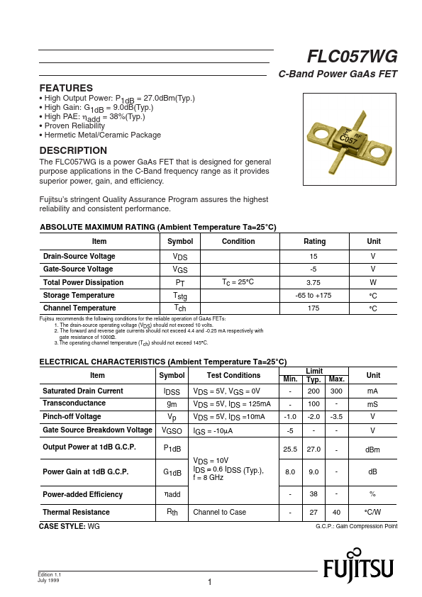
- Hermetic Metal/Ceramic Package
C-Band Power Ga As FET
DESCRIPTION
The FLC057WG is a power Ga As FET that is designed for general purpose applications in the C-Band frequency range as it provides superior power, gain, and efficiency.
Fujitsu’s stringent Quality Assurance Program assures the highest reliability and consistent performance.
ABSOLUTE MAXIMUM RATING (Ambient Temperature Ta=25°C)
Item
Symbol
Condition
Drain-Source Voltage Gate-Source Voltage
VDS VGS
Total Power Dissipation
PT Tc = 25°C
Storage Temperature Channel Temperature
Tstg Tch
Fujitsu remends the following conditions for the reliable operation of Ga As FETs:
1. The drain-source operating voltage (VDS) should not exceed 10 volts. 2. The forward and reverse gate currents should not exceed 4.4 and -0.25 m A respectively with gate resistance of 1000Ω. 3. The operating channel temperature (Tch) should not exceed 145°C.
Rating
15 -5 3.75 -65 to +175 175
Unit
V V W °C °C
ELECTRICAL CHARACTERISTICS (Ambient Temperature Ta=25°C)
Item
Symbol
Test Conditions
Min.
Saturated Drain Current Transconductance
IDSS gm
VDS = 5V, VGS = 0V VDS = 5V, IDS = 125m A
- Pinch-off Voltage
Vp
Gate Source Breakdown Voltage VGSO
VDS = 5V, IDS =10m A IGS = -10µA
-1.0 -5
Limit Typ. Max. 200 300...