MBM29DL161BE-12 Description
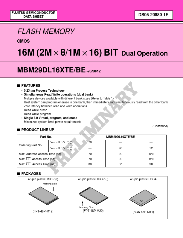
.. FUJITSU SEMICONDUCTOR DATA SHEET DS05-20880-1E FLASH MEMORY CMOS 16M (2M × 8/1M × 16) BIT Dual Operation MBM29DL16XTE/BE -70/90/12.
MBM29DL161BE-12 Key Features
- 0.23 µm Process Technology
- Simultaneous Read/Write operations (dual bank)
- Single 3.0 V read, program, and erase
- 90 12 70 90 120 70 90 120 30 35 50