Datasheet4U.com
🌙
MBM29DL163BD-90 Datasheet | Fujitsu Semiconductor Limited
Part:
MBM29DL163BD-90
Description:
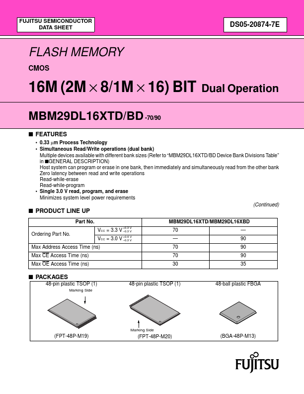
FLASH MEMORY CMOS 16M (2M x 8/1M x 16) BIT
Manufacturer:
Fujitsu Semiconductor Limited
Size:
1.10 MB
MBM29DL163BD-90 Datasheet (PDF) Download
Fujitsu Semiconductor Limited
MBM29DL163BD-90
Key Features
0.33 µm Process Technology
×
Close