MBM29F002BC-90 Description
FUJITSU SEMICONDUCTOR DATA SHEET FLASH MEMORY CMOS 2M (256K × 8) BIT DS05-20868-3E MBM29F002TC-55/-70/-90/MBM29F002BC-55/-70/-90.
MBM29F002BC-90 Key Features
- Single 5.0 V read, write, and erase Minimizes system level power requirements
- patible with JEDEC-standard mands Pinout and software patible with single-power supply Flash Superior inadvertent write
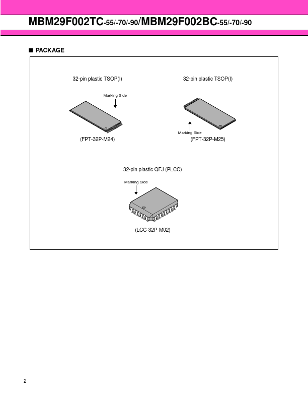
- 32-pin TSOP(I) (Package Suffix: PFTN-Normal Bend Type, PFTR-Reverse Bend Type) 32-pin PLCC (Package Suffix: PD)
- Minimum 100,000 write/erase cycles
- High performance
- Sector erase architecture
- Boot Code Sector Architecture T = Top sector B = Bottom sector
- Embedded Erase™ Algorithms Automatically pre-programs and erases the chip or any sector
- Embedded Program™ Algorithms Automatically programs and verifies data at specified address