MBM29DL163TD - (MBM29DL16xTD/BD) FLASH MEMORY CMOS 16M (2M X 8/1M X 16) BIT
Fujitsu Semiconductor Limited
Download the MBM29DL163TD datasheet PDF.
This datasheet also covers the MBM29DL16xTD variant, as both devices belong to the same (mbm29dl16xtd/bd) flash memory cmos 16m (2m x 8/1m x 16) bit family and are provided as variant models within a single manufacturer datasheet.
General Description
Host system can program or erase in one bank, then immediately and simultaneously read from the other bank Zero latency between read and write operations Read-while-erase Read-while-program
Single 3.0 V read, program, and erase Minimizes system level power requirements (Continued)
s PROD
Key Features
Dual Operation.
0.33 µm Process Technology.
Simultaneous Read/Write operations (dual bank) Multiple devices available with different bank sizes (Refer to “MBM29DL16XTD/BD Device Bank Divisions Table” in sGENERAL.
Note: The manufacturer provides a single datasheet file (MBM29DL16xTD_FujitsuMediaDevices.pdf) that lists specifications for multiple related part numbers.
Full PDF Text Transcription for MBM29DL163TD (Reference)
Note: Below is a high-fidelity text extraction (approx. 800 characters) for
MBM29DL163TD. For precise diagrams, and layout, please refer to the original PDF.
www.DataSheet4U.com FUJITSU SEMICONDUCTOR DATA SHEET DS05-20874-7E FLASH MEMORY CMOS 16M (2M × 8/1M × 16) BIT MBM29DL16XTD/BD -70/90 s FEATURES Dual Operation • 0.33 µm P...
View more extracted text
× 16) BIT MBM29DL16XTD/BD -70/90 s FEATURES Dual Operation • 0.33 µm Process Technology • Simultaneous Read/Write operations (dual bank) Multiple devices available with different bank sizes (Refer to “MBM29DL16XTD/BD Device Bank Divisions Table” in sGENERAL DESCRIPTION
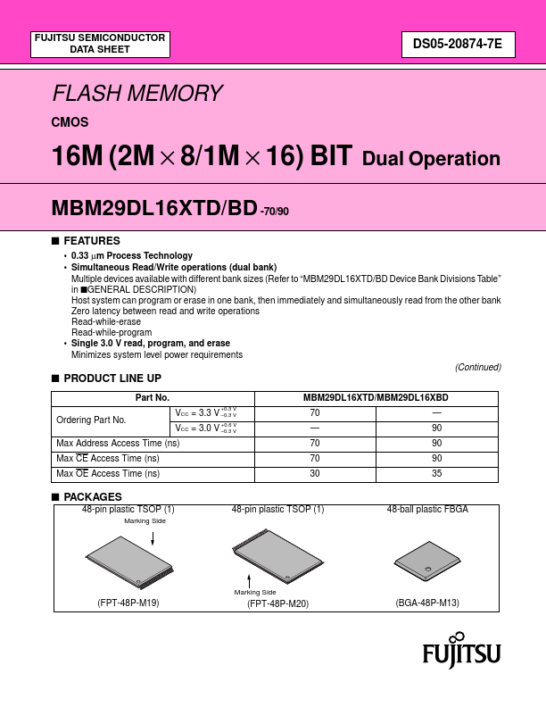
) Host system can program or erase in one bank, then immediately and simultaneously read from the other bank Zero latency between read and write operations Read-while-erase Read-while-program • Single 3.0 V read, program, and erase Minimizes system level power requirements (Continued) s PRODUCT LINE UP Part No. Ordering Part No. VCC = 3.3 V VCC = 3.0 V +0.3 V