MBM29DL323BE
Key Features
- 0.23 µm Process Technology
- Simultaneous Read/Write operations (dual bank) Multiple devices available with different bank sizes (Refer to “MBM29DL32XTE/BE Device Bank Divisions” in “s FEATURES”) Host system can program or erase in one bank, then immediately and simultaneously read from the other bank Zero latency between read and write operations Read-while-erase Read-while-program
- Single 3.0 V read, program, and erase Minimizes system level power requirements
- Compatible with JEDEC-standard commands Uses same software commands as E2PROMs
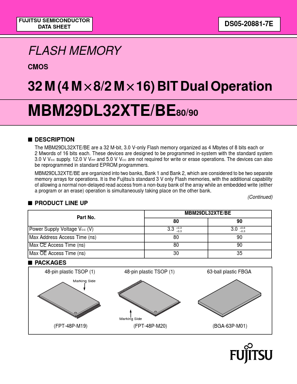
- Compatible with JEDEC-standard world-wide pinouts 48-pin TSOP (1) (Package suffix : TN - Normal Bend Type, TR - Reversed Bend Type) 63-ball FBGA (Package suffix : PBT)
- Minimum 100,000 program/erase cycles
- High performance 80 ns maximum access time
- Sector erase architecture Eight 4 Kword and sixty-three 32 Kword sectors in word mode Eight 8 Kbyte and sixty-three 64 Kbyte sectors in byte mode Any combination of sectors can be concurrently erased. Also supports full chip erase.
- Boot Code Sector Architecture T = Top sector B = Bottom sector
- HiddenROM region 64 Kbyte of HiddenROM, accessible through a new “HiddenROM Enable” command sequence Factory serialized and protected to provide a secure electronic serial number (ESN)