MBM29DL64DF
MBM29DL64DF is FLASH MEMORY CMOS 64M (8 M x 8/4 M x 16) BIT manufactured by Fujitsu Semiconductor Limited.
DESCRIPTION
MBM29DL64DF is a 64 M-bit, 3.0 V-only Flash memory organized as 8 Mbytes of 8 bits each or 4 M words of 16 bits each. The device es in 48-pin TSOP (1) and 48-ball FBGA packages. This device is designed to be programmed in system with 3.0 V VCC supply. 12.0 V VPP and 5.0 V VCC are not required for write or erase operations. The device can also be reprogrammed in standard EPROM programmers. The device is organized into four physical banks : Bank A, Bank B, Bank C and Bank D, which are considered to be four separate memory arrays operations. This device is the almost identical to Fujitsu’s standard 3 V only Flash memories, with the additional capability of allowing a normal non-delayed read access from a non-busy bank of the array while an embedded write (either a program or an erase) operation is simultaneously taking place on the other bank. (Continued) s PRODUCT LINE UP
Part No. Power Supply Voltage VCC (V) Max Address Access Time (ns) Max CE Access Time (ns) Max OE Access Time (ns) MBM29DL64DF-70
+0.6 V 3.0 V
- 0.3 V
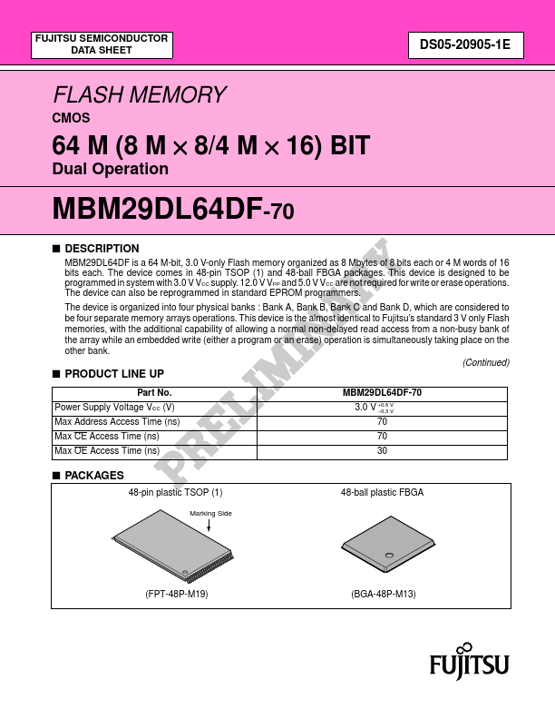
70 70 30 s PACKAGES
48-pin plastic TSOP (1)
Marking Side
48-ball plastic FBGA
(FPT-48P-M19)
(BGA-48P-M13)
MBM29DL64DF-70
(Continued)
The new design concept called Flex Bank TM
- 1 Architecture is implemented. With this concept the device can execute simultaneous operation between Bank 1, a bank chosen from among the four banks, and Bank 2, a bank consisting of the three remaining banks. This means that any bank can be chosen as Bank 1. (Refer to s FUNCTIONAL DESCRIPTION for Simultaneous Operation.) The standard device offers access times 70 ns, allowing operation of high-speed microprocessors without the wait. To eliminate bus contention the device has separate chip enable (CE) , write enable (WE) and output enable (OE) controls. This device supports pin and mand set patible with JEDEC standard E2PROMs. mands are written to the mand register using standard microprocessor write timings. Register contents serve as input to an internal...