Datasheet4U Logo Datasheet4U.com

MBM29SL800BD - FLASH MEMORY 8M (1M x 8/512K x 16) BIT

Download the MBM29SL800BD datasheet PDF. This datasheet also covers the MBM29SL800TD variant, as both devices belong to the same flash memory 8m (1m x 8/512k x 16) bit family and are provided as variant models within a single manufacturer datasheet.

General Description

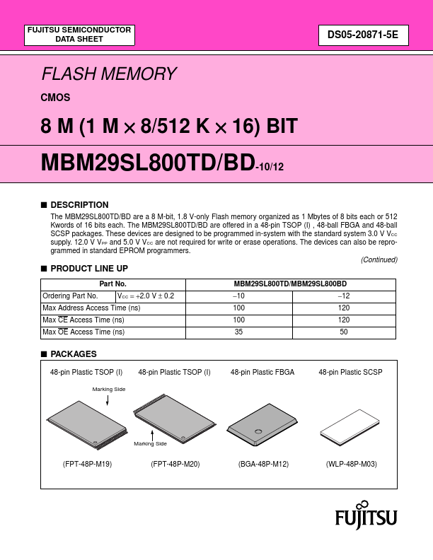
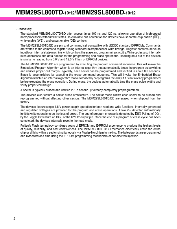
The MBM29SL800TD/BD are a 8 M-bit, 1.8 V-only Flash memory organized as 1 Mbytes of 8 bits each or 512 Kwords of 16 bits each.

The MBM29SL800TD/BD are offered in a 48-pin TSOP (I) , 48-ball FBGA and 48-ball SCSP packages.

Key Features

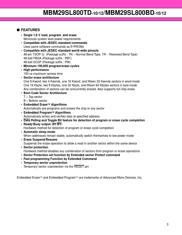
  • Single 1.8 V read, program, and erase Minimizes system level power requirements.
  • Compatible with JEDEC-standard commands Uses same software commands as E2PROMs.
  • Compatible with JEDEC-standard world-wide pinouts 48-pin TSOP (I) (Package suffix : TN.
  • Normal Bend Type, TR.
  • Reversed Bend Type) 48-ball FBGA (Package suffix : PBT) 48-ball SCSP (Package suffix : PW).
  • Minimum 100,000 program/erase cycles.
  • High performance 100 ns maximum acc.

📥 Download Datasheet

Note: The manufacturer provides a single datasheet file (MBM29SL800TD_FujitsuMediaDevices.pdf) that lists specifications for multiple related part numbers.

Full PDF Text Transcription for MBM29SL800BD (Reference)

Note: Below is a high-fidelity text extraction (approx. 800 characters) for MBM29SL800BD. For precise diagrams, and layout, please refer to the original PDF.

www.DataSheet4U.com FUJITSU SEMICONDUCTOR DATA SHEET DS05-20871-5E FLASH MEMORY CMOS 8 M (1 M × 8/512 K × 16) BIT MBM29SL800TD/BD-10/12 s DESCRIPTION The MBM29SL800TD/BD ...

View more extracted text
2 K × 16) BIT MBM29SL800TD/BD-10/12 s DESCRIPTION The MBM29SL800TD/BD are a 8 M-bit, 1.8 V-only Flash memory organized as 1 Mbytes of 8 bits each or 512 Kwords of 16 bits each. The MBM29SL800TD/BD are offered in a 48-pin TSOP (I) , 48-ball FBGA and 48-ball SCSP packages. These devices are designed to be programmed in-system with the standard system 3.0 V VCC supply. 12.0 V VPP and 5.0 V VCC are not required for write or erase operations. The devices can also be reprogrammed in standard EPROM programmers. (Continued) s PRODUCT LINE UP Part No. Ordering Part No. VCC = +2.0 V ± 0.