GS331
GS331 is LOW POWER LOW OFFSET VOLTAGE SINGLE COMPARATOR manufactured by GAINSIL.
Features l Wide Supply Voltage Range l Single Supply: 2.0V to 36V l Dual Supplies: ±1.0V to ±18V l Low Supply Current at VCC=5V: 0.4m A l Low Input Bias Current: 25n A (Typ) l Low Input Offset Current: 5n A (Typ) l Low Input Offset Voltage: ±1m V (Typ) l Input mon Mode Voltage Range Includes
Ground l Differential Input Voltage Range Equals to the Power Supply Voltage l Low Output Saturation Voltage: 200m V at 4m A l Open Collector Output l Small Package:
GS331 Available in SOT23-5 Package
General Description
The GS331 consists of a single precision voltage -parator with a typical input offset voltage of 1.0m V and high voltage gain. It is specifically designed to operate from a single power supply over wide range of voltages. Operation from split power supply is also possible and the low power supply current drain is independent of the magnitude of the power supply voltage. The GS331 is available in standard SOT-23-5 package.
Applications l Battery Charger l Cordless Telephone l Switching Power Supply
Pin Configuration l DC-DC Module l PC Motherboard l munication Equipment
March 2020-REV_V0
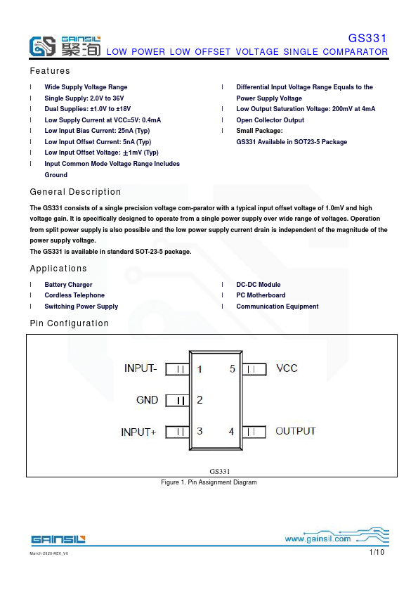
Figure 1. Pin Assignment Diagram
1/10
Functional Block Diagram
Figure 2. Functional Block Diagram of GS331
Absolute Maximum Ratings
Condition Power Supply Voltage Differential input voltage Input Voltage Operating Junction Temperature Storage Temperature Range
Symbol Vcc
VI(DIFF) VI TJ Tstg
Max ±20V or 40V
40V -0.3V~40V
150°C -65°C ~+150°C
Note 1: Stresses greater than those listed under "Absolute Maximum Ratings" may cause permanent damage to the device. These are stress ratings only, and functional operation of the device at these or any other conditions beyond those indicated under "Remended Operating Conditions" is not implied. Exposure to "Absolute Max-imum Ratings" for extended periods may affect device reliability.
Note 2: This input current will only exist when the voltage at any of the input leads is driven negative. It is due to the collector-base...