GSI Technology GS81314LT19GK
The GS81314LT19/37GK SigmaDDR-IVe ECCRAMs are synchronous devices. They employ three pairs of positive and negative input clocks; one pair of master clocks, CK and CK, and two pairs of write data clocks, KD[1:0] and KD[1:0].| Part No. | GS81314LT19GK |
|---|---|
| Datasheet | GS81314LT19GK Download |
| Manufacturer |  GSI Technology |
| Description | 144Mb SigmaDDR-IVe Burst of 2 Single-Bank ECCRAM |
| Buy | Stock & Price |
FEATURES
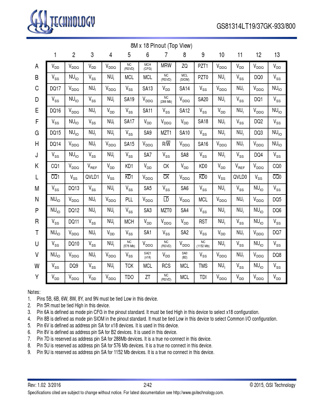
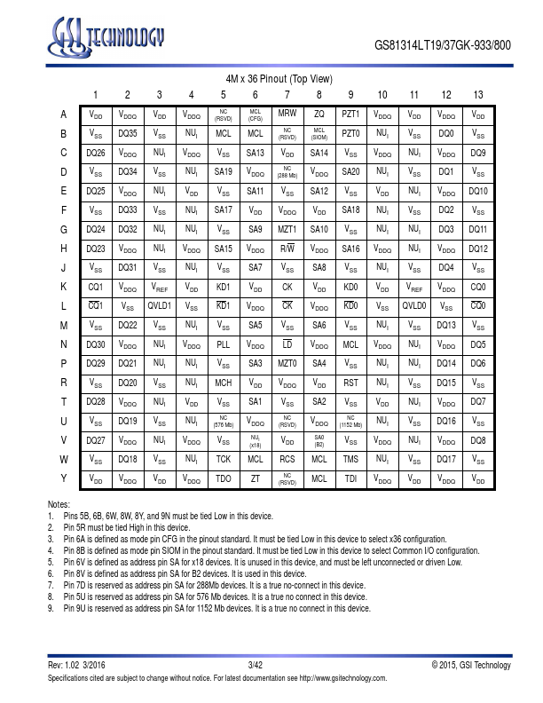
● 4Mb x 36 and 8Mb x 18 organizations available● Organized as a single logical memory bank
● 933 MHz maximum operating frequency
● 933 MT/s peak transaction rate (in millions per second)
● 67 Gb/s peak data bandwidth (in x36 devices)
● Common I/O DDR Data Bus
● Non-multiplexed SDR Address Bus
● One operation - Read or Write - per clock cycle
● No address/bank restrictions on Read and Write ops
● Burst of 2 Read and Write operations
● 5 cycle Read Latency
● On-chip ECC with virtually zero SER
● Loopback signal timing training capability
● 1.2V ~ 1.3V nominal core voltage
● 1.2V ~ 1.3V HSTL I/O interface
● Configuration registers
● Configurable ODT (on-die termination)
● ZQ pin for programmable driver impedance
● ZT pin for programmable ODT impedance
● IEEE 1149.1 JTAG-compliant Boundary Scan
● 260-pin, 14 mm x 22 mm, 1 mm ball pitch, 6/6 RoHS- compliant BGA package SigmaDDR-IVe™ Family Overview SigmaDDR-IVe ECCRAMs are the Common I/O half of the SigmaQuad-IVe/SigmaDDR-IVe family of high performance ECCRAMs.