Datasheet4U Logo Datasheet4U.com

GS8170DW36AC-350 - (GS8170DW36AC / GS8170DW72AC) Double Late Write SigmaRAM

Download the GS8170DW36AC-350 datasheet PDF. This datasheet also covers the GS8170DW36AC variant, as both devices belong to the same (gs8170dw36ac / gs8170dw72ac) double late write sigmaram family and are provided as variant models within a single manufacturer datasheet.

General Description

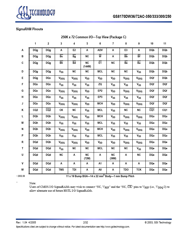
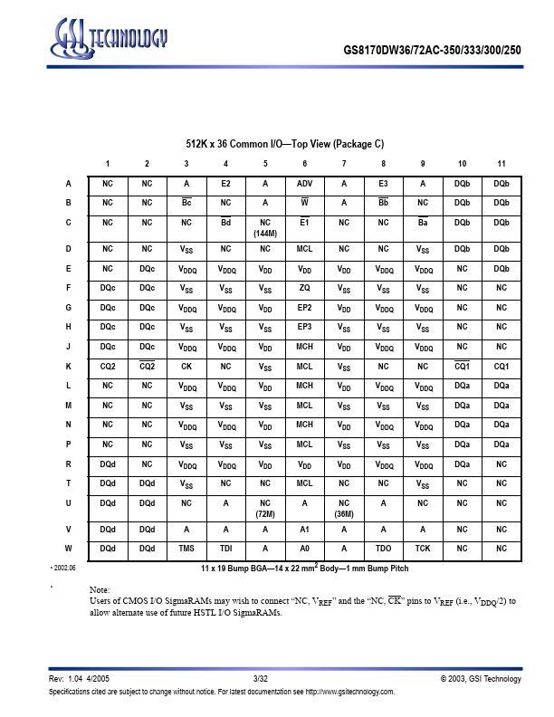
Because SigmaRAMs are synchronous devices, address data inputs and read/write control inputs are captured on the rising edge of the input clock.

Write cycles are internally self-timed and initiated by the rising edge of the clock input.

Key Features

  • Double Late Write mode, Pipelined Read mode.
  • JEDEC-standard SigmaRAM™ pinout and package.
  • 1.8 V +150/.
  • 100 mV core power supply.
  • 1.8 V CMOS Interface.
  • ZQ controlled user-selectable output drive strength.
  • Dual Cycle Deselect.
  • Burst Read and Write option.
  • Fully coherent read and write pipelines.
  • Echo Clock outputs track data output drivers.
  • Byte write operation (9-bit bytes).
  • 2 user-programma.

📥 Download Datasheet

Note: The manufacturer provides a single datasheet file (GS8170DW36AC_GSITechnology.pdf) that lists specifications for multiple related part numbers.

Datasheet Details

Part number GS8170DW36AC-350
Manufacturer GSI Technology
File Size 1.08 MB
Description (GS8170DW36AC / GS8170DW72AC) Double Late Write SigmaRAM
Datasheet download datasheet GS8170DW36AC-350 Datasheet

Full PDF Text Transcription (Reference)

The following content is an automatically extracted verbatim text from the original manufacturer datasheet and is provided for reference purposes only.

View original datasheet text
GS8170DW36/72AC-350/333/300/250 209-Bump BGA Commercial Temp Industrial Temp Features • Double Late Write mode, Pipelined Read mode • JEDEC-standard SigmaRAM™ pinout and package • 1.8 V +150/–100 mV core power supply • 1.8 V CMOS Interface • ZQ controlled user-selectable output drive strength • Dual Cycle Deselect • Burst Read and Write option • Fully coherent read and write pipelines • Echo Clock outputs track data output drivers • Byte write operation (9-bit bytes) • 2 user-programmable chip enable inputs • IEEE 1149.1 JTAG-compliant Serial Boundary Scan • 209-bump, 14 mm x 22 mm, 1 mm bump pitch BGA package • Pin-compatible with future 36Mb, 72Mb, and 144Mb devices • Pb-Free 209-bump BGA package available 18Mb Σ1x1Dp CMOS I/O Double Late Write SigmaRAM™ 250 MHz–350 MHz 1.8 V VDD 1.