GS8170LW72C-300 Overview
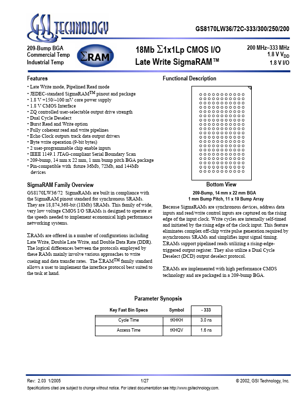
200 MHz 333 MHz 1.8 V VDD 1.8 V I/O SigmaRAM Family Overview GS8170LW36/72 SigmaRAMs are built in pliance with the SigmaRAM pinout standard for synchronous SRAMs. They are 18,874,368-bit (18Mb) SRAMs. This family of wide, very low voltage CMOS I/O SRAMs is designed to operate at the speeds needed to implement economical high performance networking systems.
GS8170LW72C-300 Key Features
- Late Write mode, Pipelined Read mode
- JEDEC-standard SigmaRAM™ pinout and package
- 1.8 V +150/-100 mV core power supply
- 1.8 V CMOS Interface
- ZQ controlled user-selectable output drive strength
- Dual Cycle Deselect
- Burst Read and Write option
- Fully coherent read and write pipelines
- Echo Clock outputs track data output drivers
- Byte write operation (9-bit bytes)