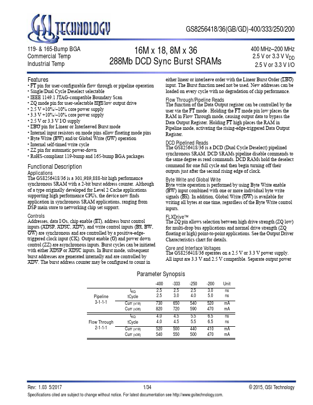
Datasheet4U Logo Datasheet4U.com

GS8256418GD-200 - 288Mb DCD Sync Burst SRAM

Download the GS8256418GD-200 datasheet PDF. This datasheet also covers the GS8256418GB-400 variant, as both devices belong to the same 288mb dcd sync burst sram family and are provided as variant models within a single manufacturer datasheet.

📥 Download Datasheet

Note: The manufacturer provides a single datasheet file (GS8256418GB-400-GSITechnology.pdf) that lists specifications for multiple related part numbers.

Datasheet Details

Part number GS8256418GD-200
Manufacturer GSI Technology
File Size 405.66 KB
Description 288Mb DCD Sync Burst SRAM
Datasheet download datasheet GS8256418GD-200 Datasheet

General Description

Applications The GS8256418/36 is a 301,989,888-bit high performance synchronous SRAM with a 2-bit burst address counter.

Although of a type originally developed for Level 2 Cache applications supporting high performance CPUs, the device now finds application in synchronous SRAM applications, ranging from DSP main store to networking chip set support.

Controls Addresses, data I/Os, chip enable (E1), address burst control inputs (ADSP, ADSC, ADV), and write control inputs (Bx, BW, GW) are synchronous and are controlled by a positive-edgetriggered clock input (CK).

Overview

GS8256418/36(GB/GD)-400/333/250/200 119- & 165-Bump BGA Commercial Temp Industrial Temp 16M x 18, 8M x 36 288Mb DCD Sync Burst SRAMs 400 MHz–200 MHz 2.5 V or 3.3 V VDD 2.5 V or 3.

Key Features

  • FT pin for user-configurable flow through or pipeline operation.
  • Single/Dual Cycle Deselect selectable.
  • IEEE 1149.1 JTAG-compatible Boundary Scan.
  • ZQ mode pin for user-selectable high/low output drive.
  • 2.5 V +10%/.
  • 10% core power supply.
  • 3.3 V +10%/.
  • 10% core power supply.
  • 2.5 V or 3.3 V I/O supply.
  • LBO pin for Linear or Interleaved Burst mode.
  • Internal input resistors on mode pins allow floating mode.