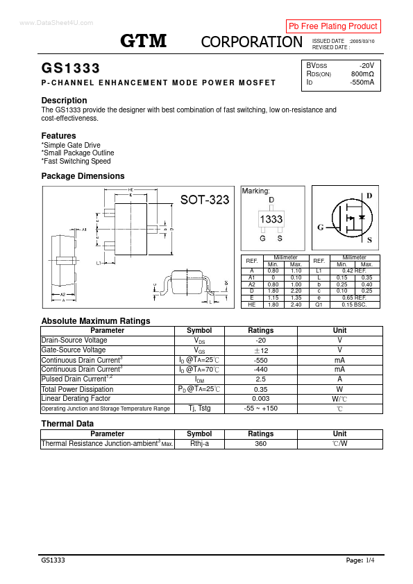
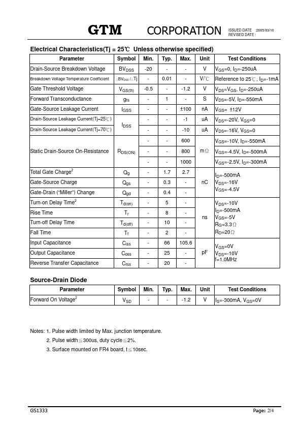
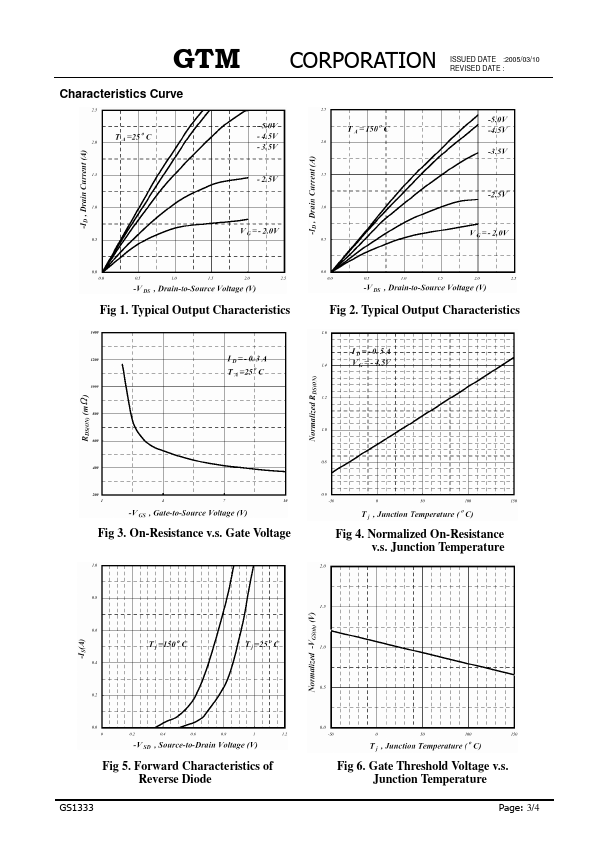
Datasheet4U Logo Datasheet4U.com

GS1333 - P-CHANNEL ENHANCEMENT MODE POWER MOSFET

General Description

The GS1333 provide the designer with best combination of fast switching, low on-resistance and cost-effectiveness.

Simple Gate Drive Small Package Outline Fast Switching Speed

Key Features

  • Package Dimensions REF. A A1 A2 D E HE Millimeter Min. Max. 0.80 1.10 0 0.10 0.80 1.00 1.80 2.20 1.15 1.35 1.80 2.40 REF. L1 L b c e Q1 Millimeter Min. Max. 0.42 REF. 0.15 0.35 0.25 0.40 0.10 0.25 0.65 REF. 0.15 BSC. Absolute Maximum Ratings Parameter Drain-Source Voltage Gate-Source Voltage Continuous Drain Current3 Continuous Drain Current3 1,2 Pulsed Drain Current Total Power Dissipation Linear Derating Factor Operating Junction and Storage Temperature Range Symbol VDS VGS ID @TA=25 ID.

📥 Download Datasheet

Datasheet Details

Part number GS1333
Manufacturer GTM
File Size 324.45 KB
Description P-CHANNEL ENHANCEMENT MODE POWER MOSFET
Datasheet download datasheet GS1333 Datasheet

Full PDF Text Transcription (Reference)

The following content is an automatically extracted verbatim text from the original manufacturer datasheet and is provided for reference purposes only.

View original datasheet text
www.DataSheet4U.com Pb Free Plating Product ISSUED DATE :2005/03/10 REVISED DATE : GS1333 P-CHANNEL ENHANCEMENT MODE POWER MOSFET BVDSS RDS(ON) ID -20V 800m -550mA Description The GS1333 provide the designer with best combination of fast switching, low on-resistance and cost-effectiveness. *Simple Gate Drive *Small Package Outline *Fast Switching Speed Features Package Dimensions REF. A A1 A2 D E HE Millimeter Min. Max. 0.80 1.10 0 0.10 0.80 1.00 1.80 2.20 1.15 1.35 1.80 2.40 REF. L1 L b c e Q1 Millimeter Min. Max. 0.42 REF. 0.15 0.35 0.25 0.40 0.10 0.25 0.65 REF. 0.15 BSC.