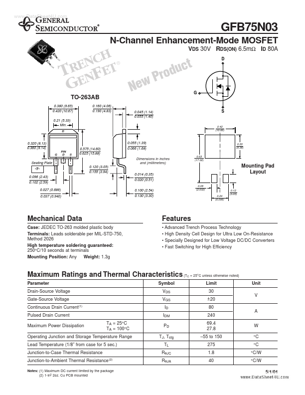
Datasheet4U Logo Datasheet4U.com

GFB75N03 - N-Channel Enhancement-Mode MOSFET

Overview

www.DataSheet4U.com GFB75N03 N-Channel Enhancement-Mode MOSFET H C N t E ET c u R d T ENF ro P G New ® VDS 30V RDS(ON) 6.5mΩ ID 80A D TO-263AB 0.380 (9.65) 0.420 (10.67) 0.21 (5.33) Min.

D G 0.160 (4.06) 0.190 (4.83) 0.045 (1.14) 0.055 (1.40) S 0.42 (10.66) 0.320 (8.13) 0.360 (9.14) G PIN D S 0.575 (14.60) 0.625 (15.88) 0.055 (1.39) 0.066 (1.68) Dimensions in inches and (millimeters) 0.63 (17.02) 0.33 (8.38) Seating Plate -T0.096 (2.43) 0.102 (2.59) 0.027 (0.686) 0.037 (0.940) 0.120 (3.05) 0.155 (3.94) 0.014 (0.35) 0.020 (0.51) 0.100 (2.54) 0.130 (3.30) 0.08 (2.032) 0.24 (6.096) 0.12 (3.05) Mounting Pad Layout Mechanical Data Case: JEDEC TO-263 molded plastic body Terminals: Leads solderable per MIL-STD-750, Method 2026 High temperature soldering guaranteed: 250°C/10 seconds at terminals Mounting Position: Any Weight: 1.

Key Features

  • Advanced Trench Process Technology.
  • High Density Cell Design for Ultra Low On-Resistance.
  • Specially Designed for Low Voltage DC/DC Converters.
  • Fast Switching for High Efficiency
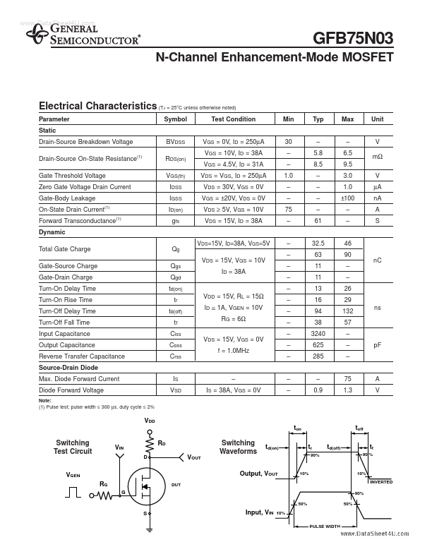
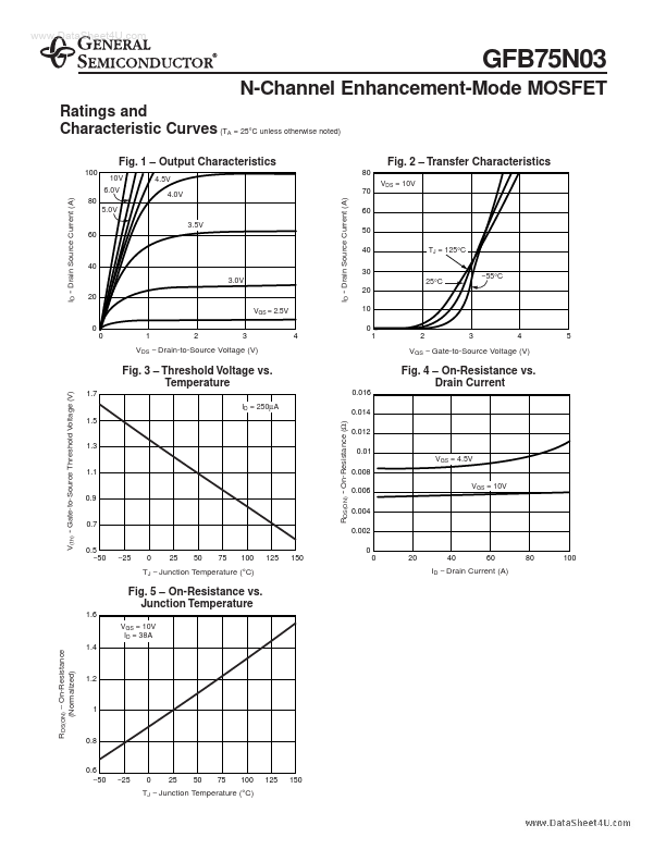
 Maximum Ratings and Thermal Characteristics (T Parameter Drain-Source Voltage Gate-Source Voltage Continuous Drain Current(1) Pulsed Drain Current Maximum Power Dissipation TA = 25°C TA = 100°C Symbol VDS VGS ID IDM PD TJ, Tstg TL RθJC (2) C = 25°C unless otherwise noted) Limit 30.