Good-Ark Semiconductor SSF6NS70UD
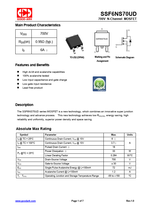
The SSF6NS70UD series MOSFET is a new technology, which combines an innovative super junction technology and advance process. This new technology achieves low RDS(ON), energy saving, high reliability and uniformity, superior power density and space saving.| Part No. | SSF6NS70UD |
|---|---|
| Datasheet | SSF6NS70UD Download |
| Manufacturer |  Good-Ark Semiconductor |
| Description | N-Channel MOSFET |
| Buy | Stock & Price |
FEATURES AND BENEFITS
● High dv/dt and avalanche capabilities● 100% avalanche tested
● Low input capacitance and gate charge
● Low gate input resistance
● Lead free product SSF6NS70UD 700V N-Channel MOSFET Marking and Pin Assignment Schematic Diagram
DESCRIPTION
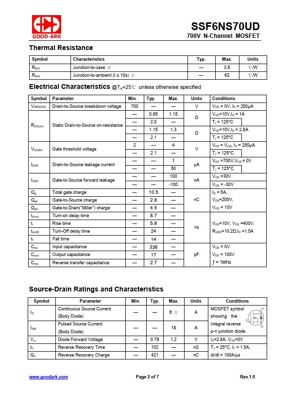
Absolute Max Rating Symbol ID @ TC = 25°C ID @ TC = 100°C IDM PD @TC = 25°C VDS VGS EAS IAS TJ TSTG Parameter Continuous Drain Current, VGS @ 10V Continuous Drain Current, VGS @ 10V Pulsed Drain Current ② Power Dissipation ③ Linear Derating Factor Drain-Source Voltage Gate-to-Source Voltage Single Pulse Avalanche Energy @ L=100mH Avalanche Current @ L=100mH Operating Junction and Storage Temperature Range Max. 6① 3.7① 18 33 0.264 700 ± 30 72 1.2 -55 to +150 Units A W W/°C V V mJ A °C Page 1 of 7 Rev.1.0 SSF6NS70UD 700V N-Channel MOSFET Thermal Resistance Symbol RθJC RθJA Characteristics Junction-to-case ③ Junction-to-ambient (t ≤ 10s) ④ Typ. — — Max. 3.8 62 Units ℃/W ℃/WELECTRICAL CHARACTERISTICS
@TA=25℃ unless otherwise spec...