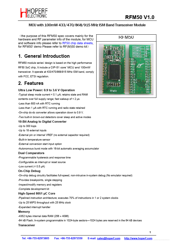
RFM50
RFM50 is MCU manufactured by HOPERF.
Features
6B
Ultra Low Power: 0.9 to 3.6 V Operation
-Typical sleep mode current < 0.1 μA; retains state and RAM contents over full supply range; fast wakeup of < 2 μs -Less than 600 n A with RTC running -Less than 1 μA with RTC running and radio state retained -On-chip dc-dc converter allows operation down to 0.9 V. -Two built-in brown-out detectors cover sleep and active modes
10-Bit Analog to Digital Converter
-Up to 300 ksps -Up to 18 external inputs -External pin or internal VREF (no external capacitor required) -Built-in temperature sensor -External conversion start input option -Autonomous burst mode with 16-bit automatic averaging accumulator
Dual parators
-Programmable hysteresis and response time -Configurable as interrupt or reset source -Low current (< 0.5 μA)
On-Chip Debug
-On-chip debug circuitry facilitates full-speed, non-intrusive in-system debug (No emulator required) -Provides breakpoints, single stepping -Inspect/modify memory and registers -plete development kit
High-Speed 8051 μC Core
-Pipelined instruction architecture; executes 70% of instructions in 1 or 2 system clocks -Up to 25 MIPS throughput with 25 MHz clock -Expanded interrupt handler
Memory
-4352 bytes internal data RAM (256 + 4096) -64 k B Flash; In-system programmable in 1024-byte sectors- 1024 bytes are reserved in the 64 k B devices
Transceiver
1 Tel: +86-755-82973805 Fax: +86-755-82973550 E-mail: sales@hoperf. http://.hoperf.
Free Datasheet http://../
RFM50 V1.0
-Frequency range = 433,470,868,915 MHz ISM Band -Sensitivity =
- 121 d Bm -FSK, GFSK, and OOK modulation -Max output power = +20 d Bm -RF power consumption
- 18.5m A receive -18 m A @+1 d Bm transmit
- 40m A @+13 d Bm transmit
- 100m A @+20 d Bm transmit -Data rate = 0.123 to 256 kbps -Auto-frequency calibration (AFC)
- transmit/receive switch control -Programmable packet handler -TX and RX 64 byte FIFOs -Frequency hopping capability -On-chip crystal tuning
Digital Peripherals
-19 or 16 port I/O plus 3 GPIO pins; Hardware...