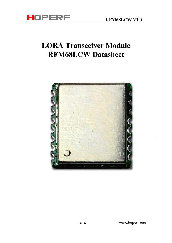
RFM68LCW Overview
Reference Design 6/ 10 .hoperf. 6 RFM68LCW V1.0 Testing Conditions:.
| Part number | RFM68LCW |
|---|---|
| Datasheet | RFM68LCW Datasheet PDF (Download) |
| File Size | 280.75 KB |
| Manufacturer | HOPERF |
| Description | LORA Transceiver |
|
|
Reference Design 6/ 10 .hoperf. 6 RFM68LCW V1.0 Testing Conditions:.