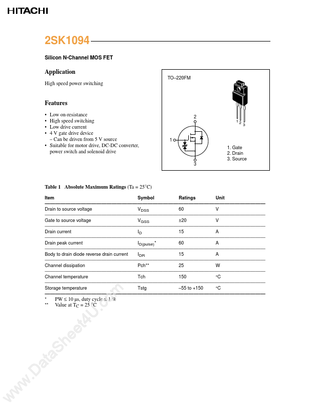
www.DataSheet4U.com
2SK1094
Table 2 Electrical Characteristics (Ta = 25°C)
Item
Symbol Min Typ Max Unit Test conditions
———————————————————————————————————————————
Drain to source breakdown
V(BR)DSS 60
—
— V ID = 10 mA, VGS = 0
voltage
———————————————————————————————————————————
Gate to source breakdown
voltage
V(BR)GSS ±20
—
— V IG = ±100 µA, VDS = 0
———————————————————————————————————————————
Gate to source leak current
IGSS
— — ±10 µA VGS = ±16 V, VDS = 0
———————————————————————————————————————————
Zero gate voltage drain current IDSS
— — 250 µA VDS = 50 V, VGS = 0
———————————————————————————————————————————
Gate to source cutoff voltage VGS(off)
1.0
—
2.0 V ID = 1 mA, VDS = 10 V
———————————————————————————————————————————
Static drain to source on state RDS(on)
resistance
—
0.055 0.065 Ω
———————
ID = 8 A, VGS = 10 V *
——————————–
0.075 0.095
ID = 8 A, VGS = 4 V *
———————————————————————————————————————————
Forward transfer admittance |yfs|
7 12 — S ID = 8 A, VDS = 10 V *
———————————————————————————————————————————
Input capacitance
Ciss
— 860 — pF VDS = 10 V, VGS = 0,
————————————————————————————————
Output capacitance
Coss
— 450 — pF f = 1 MHz
————————————————————————————————
Reverse transfer capacitance Crss
— 140 — pF
———————————————————————————————————————————
Turn-on delay time
td(on)
— 10 — ns ID = 8 A, VGS = 10 V,
————————————————————————————————
Rise time
tr — 70 — ns RL = 3.75 Ω
————————————————————————————————
Turn-off delay time
td(off)
— 180 — ns
————————————————————————————————
Fall time
tf — 120 — ns
———————————————————————————————————————————
Body to drain diode forward
voltage
VDF
— 1.3 — V IF = 15 A, VGS = 0
———————————————————————————————————————————
Body to drain diode reverse
trr
— 135 — ns IF = 15 A, VGS = 0,
recovery time
diF/dt = 50 A/µs
———————————————————————————————————————————
* Pulse Test
www.DataSheet4U.comSee characteristic curves of 2SK971.