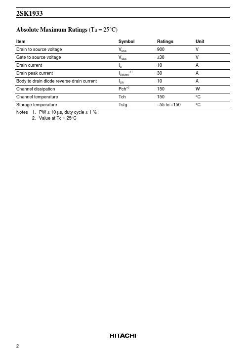
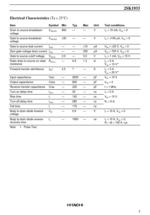
Datasheet4U Logo Datasheet4U.com

K1933 - 2SK1933

Features

  • Low on-resistance High speed switching No secondary breakdown Suitable for Switching regulator Outline TO-3P D G 1 2 3 1. Gate 2. Drain (Flange) 3. Source S 2SK1933 Absolute Maximum Ratings (Ta = 25°C) Item Drain to source voltage Gate to source voltage Drain current Drain peak current Body to drain diode reverse drain current Channel dissipation Channel temperature Storage temperature Notes 1. PW ≤ 10 µs, duty cycle ≤ 1 % 2. Value at Tc = 25°C Symbol.

📥 Download Datasheet

Datasheet preview – K1933
Other Datasheets by Hitachi Semiconductor

Full PDF Text Transcription

Click to expand full text
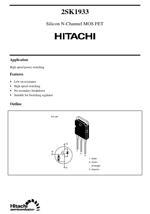
2SK1933 Silicon N-Channel MOS FET Application High speed power switching Features • • • • Low on-resistance High speed switching No secondary breakdown Suitable for Switching regulator Outline TO-3P D G 1 2 3 1. Gate 2. Drain (Flange) 3. Source S 2SK1933 Absolute Maximum Ratings (Ta = 25°C) Item Drain to source voltage Gate to source voltage Drain current Drain peak current Body to drain diode reverse drain current Channel dissipation Channel temperature Storage temperature Notes 1. PW ≤ 10 µs, duty cycle ≤ 1 % 2.
Published: |