- Part: H5TQ2G83DFR-xxC
- Manufacturer: SK Hynix
- Size: 333.13 KB
 Page 2
 Page 3
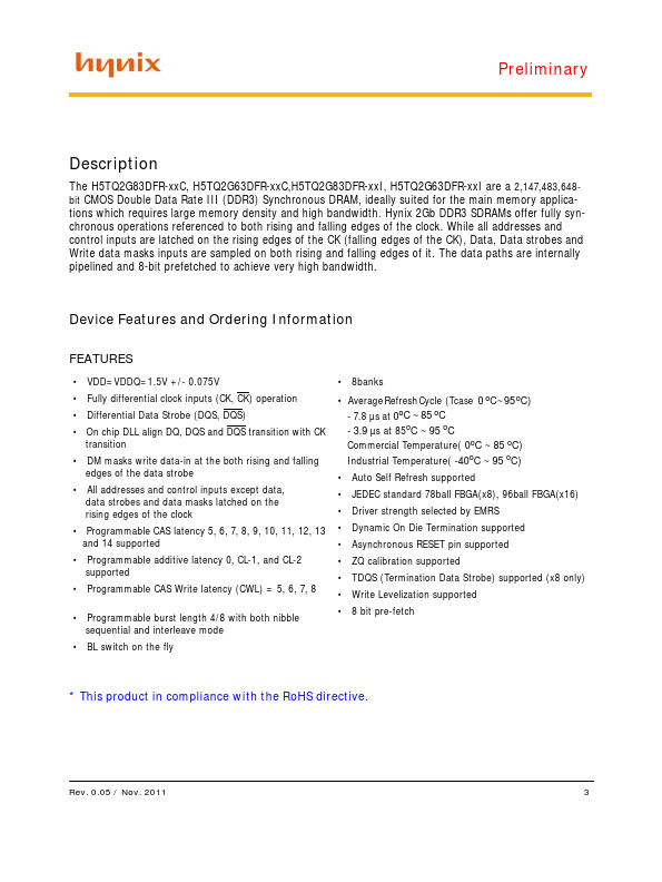
H5TQ2G83DFR-xxC Key Features
- VDD=VDDQ=1.5V +/- 0.075V
- Fully differential clock inputs (CK, CK) operation
- Differential Data Strobe (DQS, DQS)
- On chip DLL align DQ, DQS and DQS transition with CK transition
- DM masks write data-in at the both rising and falling edges of the data strobe
- All addresses and control inputs except data, data strobes and data masks latched on the rising edges of the clock
- Programmable additive latency 0, CL-1, and CL-2 supported
- Programmable CAS Write latency (CWL) = 5, 6, 7, 8
- Programmable burst length 4/8 with both nibble sequential and interleave mode
- BL switch on the fly
Related SK Hynix Datasheets