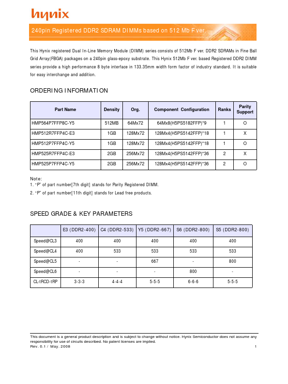
• Part: HMP512R7FFP4C-E3
  • Description: 240pin Registered DDR2 SDRAM DIMMs
  • Manufacturer: SK Hynix
  • Size: 753.52 KB
HMP512R7FFP4C-E3 Datasheet (PDF) Download
SK Hynix
HMP512R7FFP4C-E3

Key Features

  • Negative Negative line of the differential pair of system clock inputs that drives input to the on-DIMM PLL
  • Edge Active High Active Low Active High Active Low Activates the DDR2 SDRAM CK signal when high and deactivates the CK signal when low
  • By deactivating the clocks, CKE low initiates the Power Down mode or the Self Refresh mode
  • Enables the associated DDR2 SDRAM mand decoder when low and disables the mand decoder when high
  • When the mand decoder is disabled, new mands are ignored but previous operations continue
  • Rank 0 is selected by S0; Rank 1 is selected by S1 On-Die Termination signals
  • When sampled at the positive rising edge of the clock
  • RAS,CAS and WE(ALONG WITH S) define the mand being entered
  • Reference voltage for SSTL18 inputs Power supplies for the DDR2 SDRAM output buffers to provide improved noise immunity
  • For all current DDR2 unbuffered DIMM designs, VDDQ shares the same power plane as VDD pins