HMP525R7FFP4C-E3
HMP525R7FFP4C-E3 is 240pin Registered DDR2 SDRAM DIMMs manufactured by SK Hynix.
- Part of the HMP564P7FFP8C-Y5 comparator family.
- Part of the HMP564P7FFP8C-Y5 comparator family.
..net
240pin Registered DDR2 SDRAM DIMMs based on 512 Mb F ver.
This Hynix registered Dual In-Line Memory Module (DIMM) series consists of 512Mb F ver. DDR2 SDRAMs in Fine Ball Grid Array(FBGA) packages on a 240pin glass-epoxy substrate. This Hynix 512Mb F ver. based Registered DDR2 DIMM series provide a high performance 8 byte interface in 133.35mm width form factor of industry standard. It is suitable for easy interchange and addition.
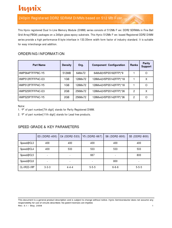
ORDERING INFORMATION
Part Name HMP564P7FFP8C-Y5 HMP512R7FFP4C-E3 HMP512P7FFP4C-Y5 HMP525R7FFP4C-E3 HMP525P7FFP4C-Y5 Density 512MB 1GB 1GB 2GB 2GB Org. 64Mx72 128Mx72 128Mx72 256Mx72 256Mx72 ponent Configuration 64Mx8(H5PS5182FFP)- 9 128Mx4(H5PS5142FFP)- 18 128Mx4(H5PS5142FFP)- 18 128Mx4(H5PS5142FFP)- 36 128Mx4(H5PS5142FFP)- 36 Ranks 1 1 1 2 2 Parity Support O X O X O
Note: 1. “P” of part number[7th digit] stands for Parity Registered DIMM. 2. “P” of part number[11th digit] stands for Lead free products.
SPEED GRADE & KEY PARAMETERS
E3 (DDR2-400) Speed@CL3 Speed@CL4 Speed@CL5 Speed@CL6 CL-t RCD-t RP 400 400 3-3-3 C4 (DDR2-533) Y5 (DDR2-667) 400 533 4-4-4 400 533 667 5-5-5 S6 (DDR2-800) 400 533 800 6-6-6 S5 (DDR2-800) 400 533 800 5-5-5
This document is a general product description and is subject to change without notice. Hynix Semiconductor does not assume any responsibility for use of circuits described. No patent licenses are implied. Rev. 0.1 / May. 2008 1
..net
1240pin Registered DDR2 SDRAM DIMMs Features
- -
- -
- -
- -
- -
- -
- -
- -
- - JEDEC standard 1.8V +/- 0.1V Power Supply VDDQ : 1.8V +/- 0.1V All inputs and outputs are patible with SSTL_1.8 interface 4 Bank architecture Posted CAS Programmable CAS Latency 3 , 4 , 5 OCD (Off-Chip Driver Impedance Adjustment) ODT (On-Die Termination) Fully differential clock operations (CK & CK) Programmable Burst Length 4 / 8 with both sequential and interleave mode Average Auto Refresh Period 7.8us under TCASE 85℃, 3.9us at 85℃ < TCASE ≤ 95 ℃ High...