Datasheet Summary
..net
240pin Registered DDR2 SDRAM DIMMs based on 512 Mb F ver.
This Hynix registered Dual In-Line Memory Module (DIMM) series consists of 512Mb F ver. DDR2 SDRAMs in Fine Ball Grid Array(FBGA) packages on a 240pin glass-epoxy substrate. This Hynix 512Mb F ver. based Registered DDR2 DIMM series provide a high performance 8 byte interface in 133.35mm width form factor of industry standard. It is suitable for easy interchange and addition.
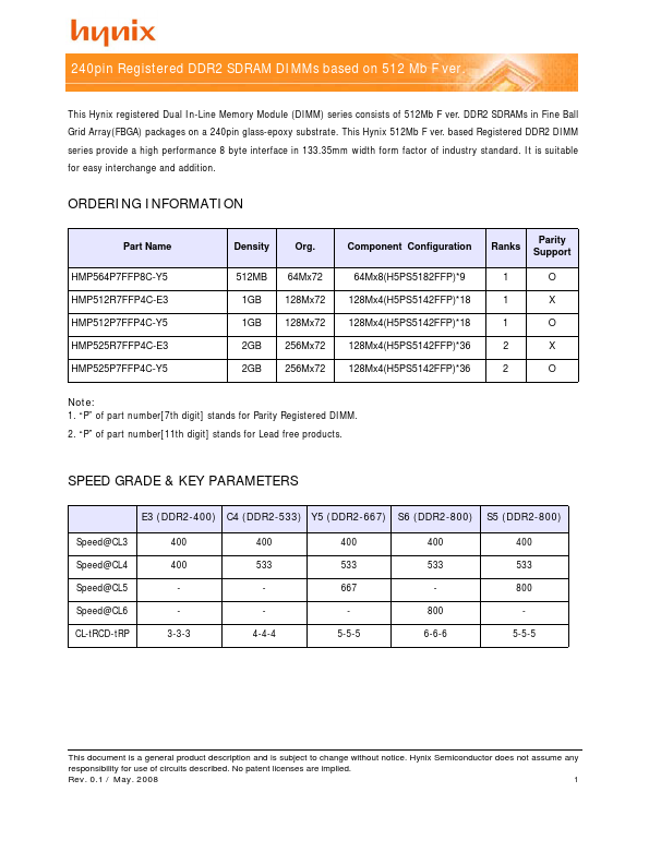
ORDERING INFORMATION
Part Name HMP564P7FFP8C-Y5 HMP512R7FFP4C-E3 HMP512P7FFP4C-Y5 HMP525R7FFP4C-E3 HMP525P7FFP4C-Y5 Density 512MB 1GB 1GB 2GB 2GB Org. 64Mx72 128Mx72 128Mx72 256Mx72 256Mx72 ponent Configuration 64Mx8(H5PS5182FFP)- 9...