HY5DU561622AT Overview
and is subject to change without notice. Hynix semiconductor does not assume any responsibility for use of circuits described. No patent licenses are implied.
HY5DU561622AT Key Features
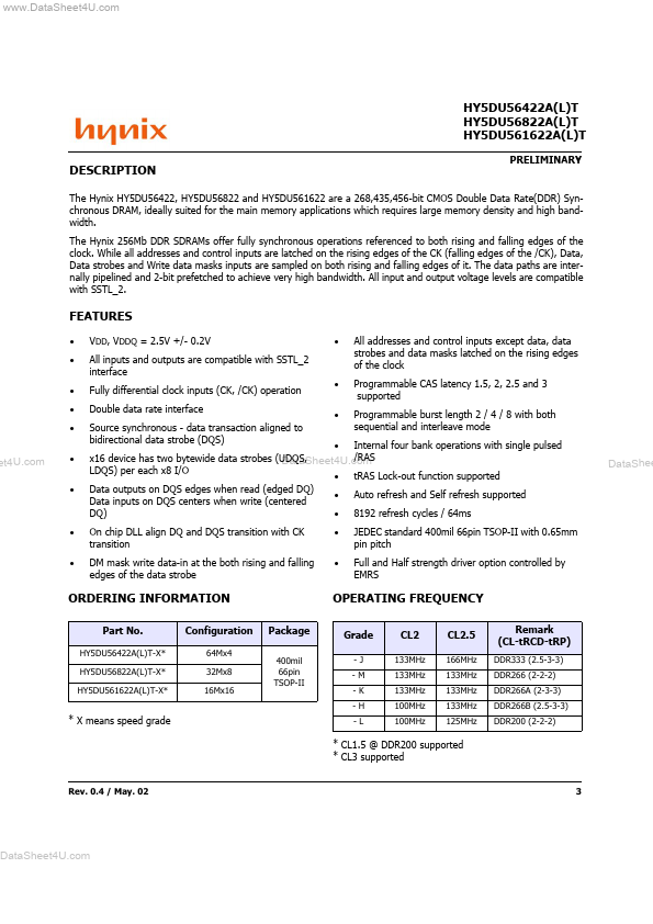
- VDD, VDDQ = 2.5V +/- 0.2V All inputs and outputs are patible with SSTL_2 interface Fully differential clock inputs (CK,
- data transaction aligned to bidirectional data strobe (DQS)
- All addresses and control inputs except data, data strobes and data masks latched on the rising edges of the clock Progr
- Internal four bank operations with single pulsed /RAS x16 device has two bytewide data strobes (UDQS, . LDQS) per each x
- tRAS Lock-out function supported Data outputs on DQS edges when read (edged DQ)
- Auto refresh and Self refresh supported Data inputs on DQS centers when write (centered DQ)
- 8192 refresh cycles / 64ms On chip DLL align DQ and DQS transition with CK transition DM mask write data-in at the both
- JEDEC standard 400mil 66pin TSOP-II with 0.65mm pin pitch Full and Half strength driver option controlled by EMRS