Datasheet4U Logo Datasheet4U.com

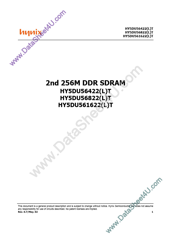
HY5DU56822T - (HY5DU56xxx(L)T) 2nd 256M DDR SDRAM

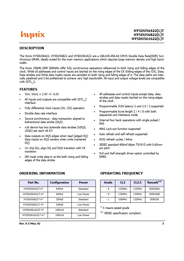
Description

and is subject to change without notice.

Hynix Semiconductor Inc.

does not assume any responsibility for use of circuits described.

Features

  • VDD, VDDQ = 2.5V +/- 0.2V All inputs and outputs are compatible with SSTL_2 interface Fully differential clock inputs (CK, /CK) operation Double data rate interface Source synchronous - data transaction aligned to bidirectional data strobe (DQS) x16 device has two bytewide data strobes (UDQS, LDQS) per each x8 I/O Data outputs on DQS edges when read (edged DQ) Data inputs on DQS centers when write (centered DQ) On chip DLL ali.

📥 Download Datasheet

Datasheet preview – HY5DU56822T

Datasheet Details

Part number HY5DU56822T
Manufacturer SK Hynix
File Size 370.15 KB
Description (HY5DU56xxx(L)T) 2nd 256M DDR SDRAM
Datasheet download datasheet HY5DU56822T Datasheet
Additional preview pages of the HY5DU56822T datasheet.
Other Datasheets by Hynix Semiconductor

Full PDF Text Transcription

Click to expand full text
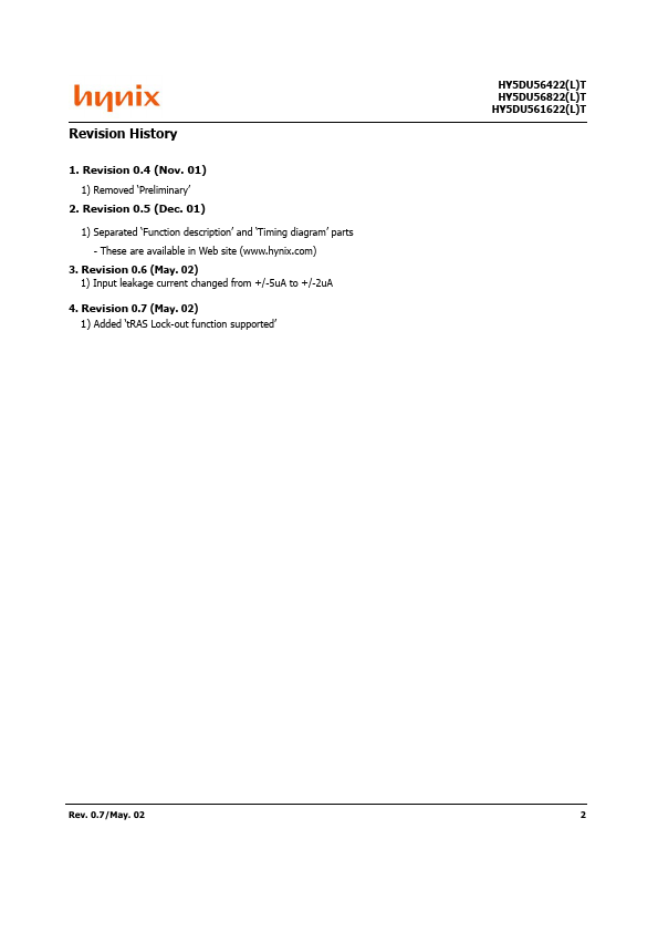
m o .c U 4 t e e h S a at .D w w w HY5DU56422(L)T HY5DU56822(L)T HY5DU561622(L)T m 2nd 256M DDR SDRAM o .c U 4 t e e h S a t a .D w w w HY5DU56422(L)T HY5DU56822(L)T HY5DU561622(L)T This document is a general product description and is subject to change without notice. Hynix Semiconductor Inc. does not assume any responsibility for use of circuits described. No patent licenses are implied. Rev. 0.7/May. 02 1 m o .c U 4 t e e h S a at .D w w w HY5DU56422(L)T HY5DU56822(L)T HY5DU561622(L)T Revision History 1. Revision 0.4 (Nov. 01) 1) Removed ‘Preliminary’ 2. Revision 0.5 (Dec. 01) 1) Separated ‘Function description’ and ‘Timing diagram’ parts - These are available in Web site (www.hynix.com) 3. Revision 0.6 (May. 02) 1) Input leakage current changed from +/-5uA to +/-2uA 4.
Published: |