HY5V26CSF Description
Preliminary The Hynix HY5V26C(L/S)F is a 134,217,728bit CMOS Synchronous DRAM, ideally suited for the main memory applications which require large memory density and high bandwidth. HY5V26C(L/S)F is organized as 4banks of 2,097,152x16 HY5V26C(L/S)F is offering fully synchronous operation referenced to a positive edge of the clock. All inputs and outputs are synchronized with the rising edge of the clock input.
HY5V26CSF Key Features
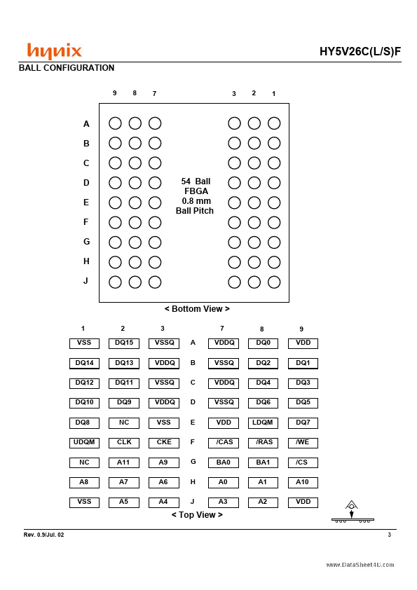
- Single 3.3±0.3V power supply All device balls are patible with LVTTL interface 54Ball FBGA (10.5mm x 8.3mm) All inputs a
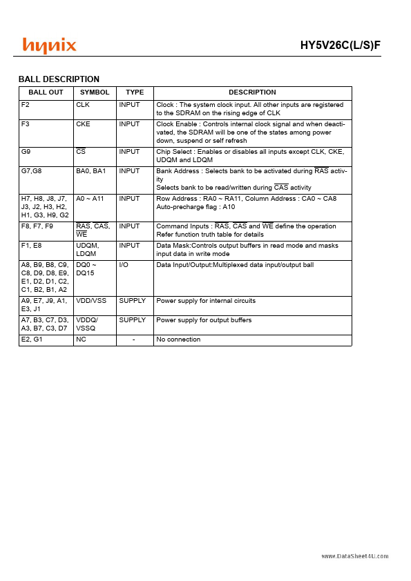
- Internal four banks operation Programmable CAS Latency ; 2, 3 Clocks
- Auto refresh and self refresh 4096 refresh cycles / 64ms Programmable Burst Length and Burst Type
- 1, 2, 4, 8 or Full page for Sequential Burst
- 1, 2, 4 or 8 for Interleave Burst
- ORDERING INFORMATION