Datasheet4U Logo Datasheet4U.com

9LPRS365 - ICS9LPRS365

Description

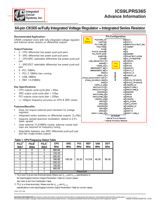
PIN # PIN NAME TYPE DESCRIPTION 3.3V PCI clock output or Clock Request control A for either SRC0 or SRC2 pair The power-up default is PCI0 output, but this pin may also be used as a Clock Request control of SRC pair 0 or SRC pair 2 via SMBus.

Features

  • 2 - CPU differential low power push-pull pairs.
  • 9 - SRC differential low power push-pull pairs.
  • 1 - CPU/SRC selectable differential low power push-pull pair.
  • 1 - SRC/DOT selectable differential low power push-pull pair.
  • 5 - PCI, 33MHz.
  • 1 - PCI_F, 33MHz free running.
  • 1 - USB, 48MHz.
  • 1 - REF, 14.318MHz Key Specifications:.
  • CPU outputs cycle-cycle jitter < 85ps.
  • SRC output cycle-cycle jitter < 125ps.

📥 Download Datasheet

Datasheet preview – 9LPRS365

Datasheet Details

Part number 9LPRS365
Manufacturer ICS
File Size 661.56 KB
Description ICS9LPRS365
Datasheet download datasheet 9LPRS365 Datasheet
Additional preview pages of the 9LPRS365 datasheet.
Other Datasheets by ICS

Full PDF Text Transcription

Click to expand full text
Integrated Circuit www.DataSheet4U.com Systems, Inc. ICS9LPRS365 Advance Information 64-pin CK505 w/Fully Integrated Voltage Regulator + Integrated Series Resistor Recommended Application: CK505 compliant clock with fully integrated voltage regulator and Internal series resistor on differential outputs Output Features: • 2 - CPU differential low power push-pull pairs • 9 - SRC differential low power push-pull pairs • 1 - CPU/SRC selectable differential low power push-pull pair • 1 - SRC/DOT selectable differential low power push-pull pair • 5 - PCI, 33MHz • 1 - PCI_F, 33MHz free running • 1 - USB, 48MHz • 1 - REF, 14.
Published: |