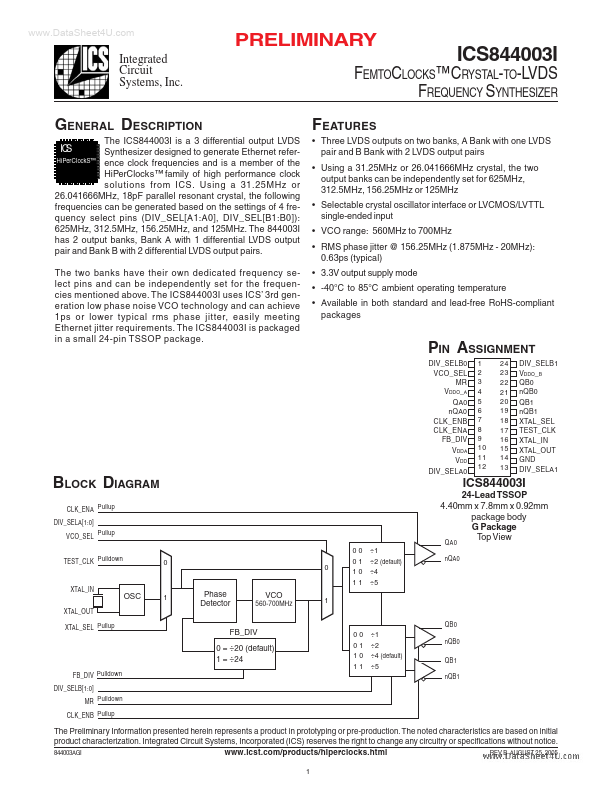
ICS844003I Key Features
- Three LVDS outputs on two banks, A Bank with one LVDS pair and B Bank with 2 LVDS output pairs
- Using a 31.25MHz or 26.041666MHz crystal, the two output banks can be independently set for 625MHz, 312.5MHz, 156.25MHz
- Selectable crystal oscillator interface or LVCMOS/LVTTL single-ended input
- VCO range: 560MHz to 700MHz
- RMS phase jitter @ 156.25MHz (1.875MHz
- 20MHz): 0.63ps (typical)
- 3.3V output supply mode
- 40°C to 85°C ambient operating temperature
- Available in both standard and lead-free RoHS-pliant packages