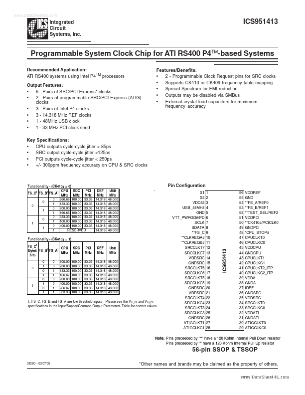
Datasheet4U Logo Datasheet4U.com

ICS951413 Datasheet - ICS

ICS951413 Programmable System Clock Chip

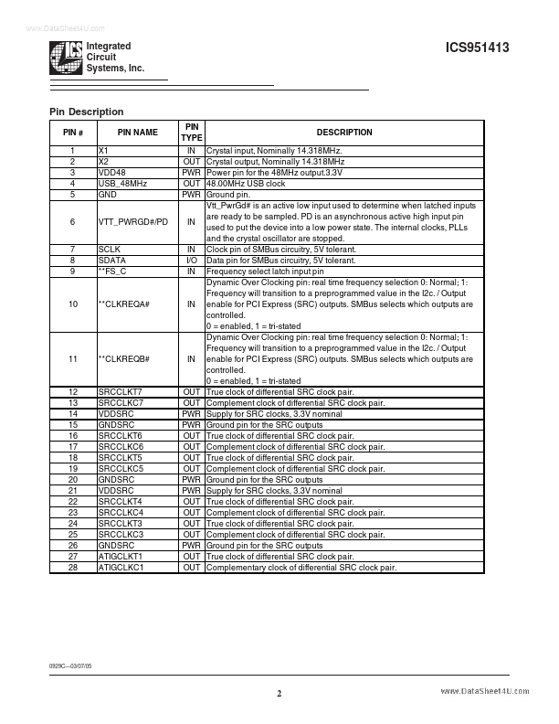
PIN # 1 2 3 4 5 6 7 8 9 PIN NAME X1 X2 VDD48 USB_48MHz GND VTT_PWRGD#/PD SCLK SDATA * *FS_C PIN TYPE IN OUT PWR OUT PWR IN IN I/O IN DESCRIPTION Crystal input, Nominally 14.318MHz. Crystal output, Nominally 14.318MHz Power pin for the 48MHz output.3.3V 48.00MHz USB clock Ground pin. Vtt_PwrGd.

ICS951413 Features

* 6 - Pairs of SRC/PCI Express

* clocks

* 2 - Pairs of programmable SRC/PCI Express (ATIG) clocks

* 3 - Pairs of Intel P4 clocks

* 3 - 14.318 MHz REF clocks

* 1 - 48MHz USB clock

* 1 - 33 MHz PCI clock seed Key Specifications:

* CPU outputs

ICS951413_ICS.pdf

Preview of ICS951413 PDF
ICS951413 Datasheet Preview Page 2 ICS951413 Datasheet Preview Page 3

Datasheet Details

Part number:

ICS951413

Manufacturer:

ICS

File Size:

355.28 KB

Description:

Programmable system clock chip.

📁 Related Datasheet

ICS951411 System Clock Chip (ICS)

ICS951412 System Clock Chip (ICS)

ICS951416 System Clock Chip (ICS)

ICS951402 Programmable Timing Control-Hub processor (ICS)

ICS951402 Programmable Timing Control-Hub processor (Renesas)

ICS951403 AMD-K7 System Clock Chip (ICS)

ICS951462 Programmable System Clock Chip (ICS)

ICS951601 General Purpose Frequency Timing Generator (Integrated Circuit Solution Inc)

TAGS

ICS951413 ICS951413 Programmable System Clock Chip ICS

ICS951413 Distributor