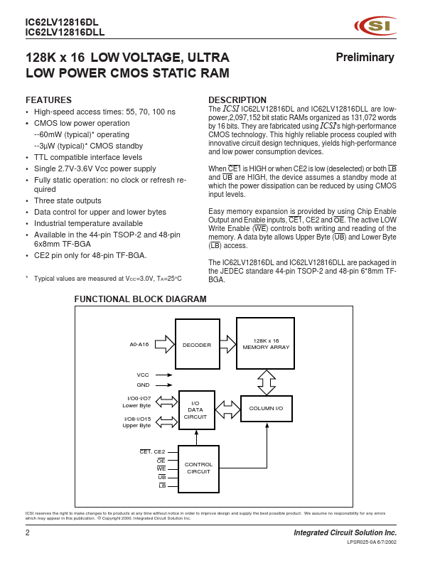
IC62LV12816DL Description
They are fabricated using ICSI's high-performance CMOS technology. This highly reliable process coupled with innovative circuit design techniques, yields high-performance and low power consumption devices. When CE1 is HIGH or when CE2 is low (deselected) or both LB and UB are HIGH, the device assumes a standby mode at which the power dissipation can be reduced by using CMOS input levels.
IC62LV12816DL Key Features
- High-speed access times: 55, 70, 100 ns
- CMOS low power operation --60mW (typical)- operating --3µW (typical)- CMOS standby
- TTL patible interface levels
- Single 2.7V-3.6V Vcc power supply
- Fully static operation: no clock or refresh required
- Three state outputs
- Data control for upper and lower bytes
- Industrial temperature available
- Available in the 44-pin TSOP-2 and 48-pin 6x8mm TF-BGA
- CE2 pin only for 48-pin TF-BGA