ICS853111-01
Overview
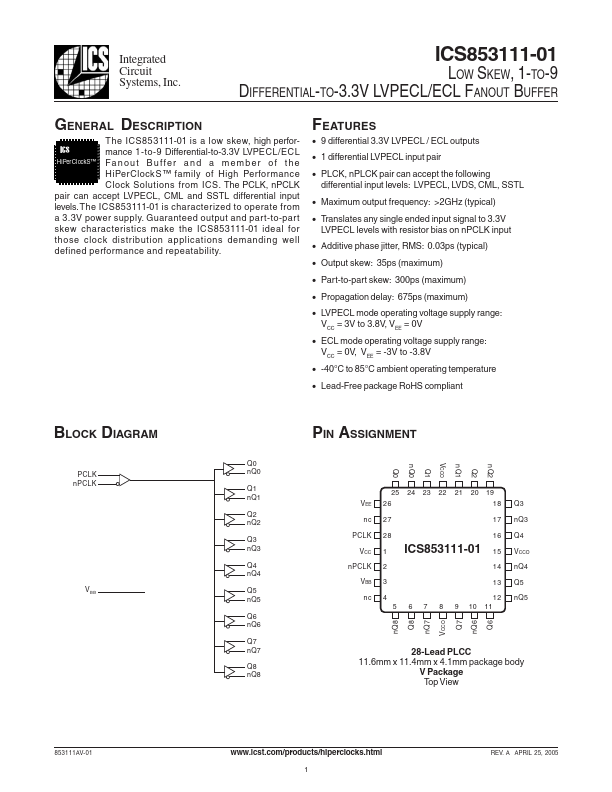
The ICS853111-01 is a low skew, high performance 1-to-9 Differential-to-3.3V LVPECL/ECL HiPerClockS™ Fa n o u t B u f fe r a n d a m e m b e r o f t h e HiPerClock S ™ family of High Performance Clock Solutions from ICS. The PCLK, nPCLK pair can accept LVPECL, CML and SSTL differential input levels.
- 9 differential 3.3V LVPECL / ECL outputs
- 1 differential LVPECL input pair
- PLCK, nPLCK pair can accept the following differential input levels: LVPECL, LVDS, CML, SSTL
- Maximum output frequency: >2GHz (typical)
- Translates any single ended input signal to 3.3V LVPECL levels with resistor bias on nPCLK input
- Additive phase jitter, RMS: 0.03ps (typical)
- Output skew: 35ps (maximum)
- Part-to-part skew: 300ps (maximum)
- Propagation delay: 675ps (maximum)
- LVPECL mode operating voltage supply range: VCC = 3V to 3.8V, VEE = 0V