M1025
Description
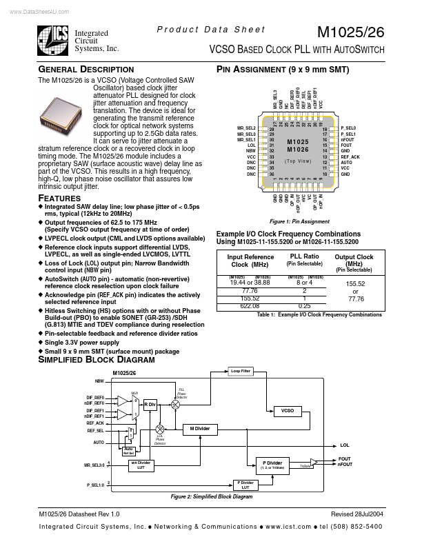
The M1025/26 is a VCSO (Voltage Controlled SAW Oscillator) based clock jitter attenuator PLL designed for clock jitter attenuation and frequency translation. The device is ideal for generating the transmit reference clock for optical network systems supporting up to 2.5Gb data rates.