8302I
8302I is 1-TO-2 LVCMOS / LVTTL FANOUT BUFFER manufactured by IDT.
DESCRIPTION
The 8302I is a low skew, 1-to-2 LVCMOS Fanout Buffer. The 8302I has a single ended clock input. The single ended clock input accepts LVCMOS or LVTTL input levels. The 8302I features a pair of LVCMOS outputs. The 8302I is characterized at full 3.3V for input VDD, and mixed 3.3V and 2.5V for output operating supply modes (VDDO). Guaranteedoutput and part-to-part skew characteristics make the 8302I ideal for clock distribution applications demanding well defined performance and repeatibility.
FEATURES
- 2 LVCMOS / LVTTL outputs
- LVCMOS / LVTTL clock input accepts LVCMOS or LVTTL input levels
- Maximum output frequency: 200MHz
- Output skew: 40ps (typical)
- Part-to-part skew: 250ps (typical)
- Small 8 lead SOIC package saves board space
- Full 3.3V or 3.3V core, 2.5V supply modes
- -40°C to 85°C ambient operating temperature
- Lead-Free package fully Ro HS pliant
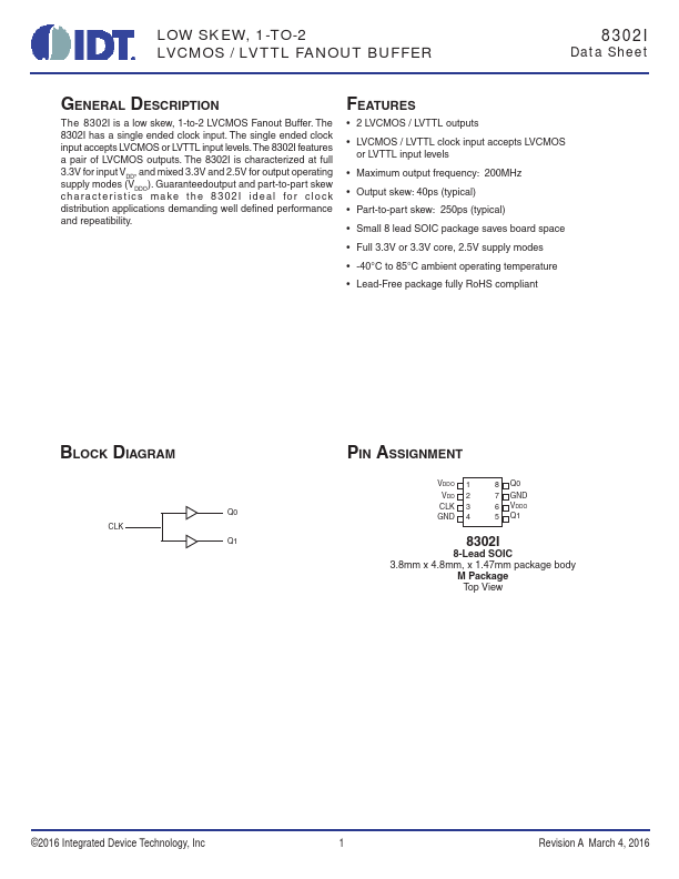
BLOCK DIAGRAM
Q0 CLK
Q1
PIN ASSIGNMENT
VDDO 1 VDD 2 CLK 3
GND 4
8 Q0 7 GND 6 VDDO 5 Q1
8-Lead SOIC 3.8mm x 4.8mm, x 1.47mm package body
M Package Top View
©2016 Integrated Device Technology, Inc
Revision A March 4, 2016
8302I Data Sheet
TABLE 1. PIN DESCRIPTIONS
Number
Name
Type
Description
1, 6
VDDO
Power
Output supply pins.
Power
Core supply pin.
Input Pulldown LVCMOS / LVTTL clock...