ICS8735I-21
Description
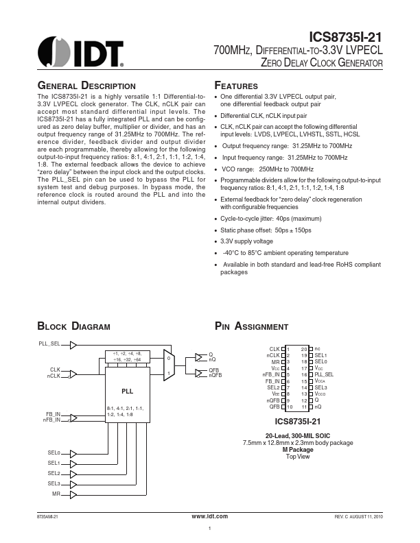
The ICS8735I-21 is a highly versatile 1:1 Differential-to3.3V LVPECL clock generator. The CLK, nCLK pair can accept most standard differential input levels.
Key Features
- One differential 3.3V LVPECL output pair, one differential feedback output pair
- Differential CLK, nCLK input pair
- CLK, nCLK pair can accept the following differential input levels: LVDS, LVPECL, LVHSTL, SSTL, HCSL
- Output frequency range: 31.25MHz to 700MHz
- Input frequency range: 31.25MHz to 700MHz
- VCO range: 250MHz to 700MHz
- External feedback for “zero delay” clock regeneration with configurable frequencies
- Cycle-to-cycle jitter: 40ps (maximum)
- Static phase offset: 50ps ± 150ps
- 3.3V supply voltage