ICS9UMS9633B Overview
Key Specifications
Mount Type: Surface Mount
Max Frequency: 166.67 MHz
Max Operating Temp: 85 °C
Min Operating Temp: -40 °C
Key Features
- Supports Dothan ULV CPUs with 67 to 167 MHz CPU outputs Dedicated TEST/SEL and TEST/MODE pins saves isolation resistors on pins CPU STOP# input for power manangment Fully integrated Vreg Integrated series resistors on differential outputs 1.5V VDD IO operation, 3.3V VDD core and REF supply pin for REF Industrial Temperature (-40 to +85C) version available
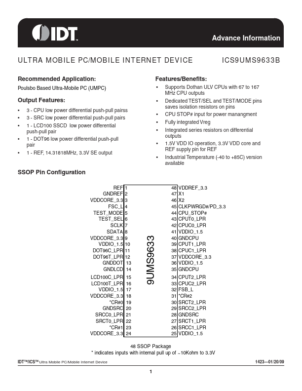
- 3 - CPU low power differential push-pull pairss 3 - SRC low power differential push-pull pairs 1 - LCD100 SSCD low power differential push-pull pair 1 - DOT96 low power differential push-pull pair 1 - REF, 14.31818MHz, 3.3V SE output